The MX55 is one of the semi-pro reel-to-reel machines made by Otari. The machine implements robust construction but the signal path is very complicated full of op-amps. This article describe the required modifications for the improvement of the playback and recording. The preliminary work is based on:
- full rebuild of the mechanism – cleaning and lubricating the mechanism;
- new brakes and new bearings for the reel motors;
- new bearings for the capstan motor
- replacement of all the electrolytic capacitors also the orange PP capacitors;
Detailed photos can be found at the official web page of the lab at:
https://www.facebook.com/media/set/?set=a.2396058583761163&type=1&l=2ba0930233
The Playback Amp
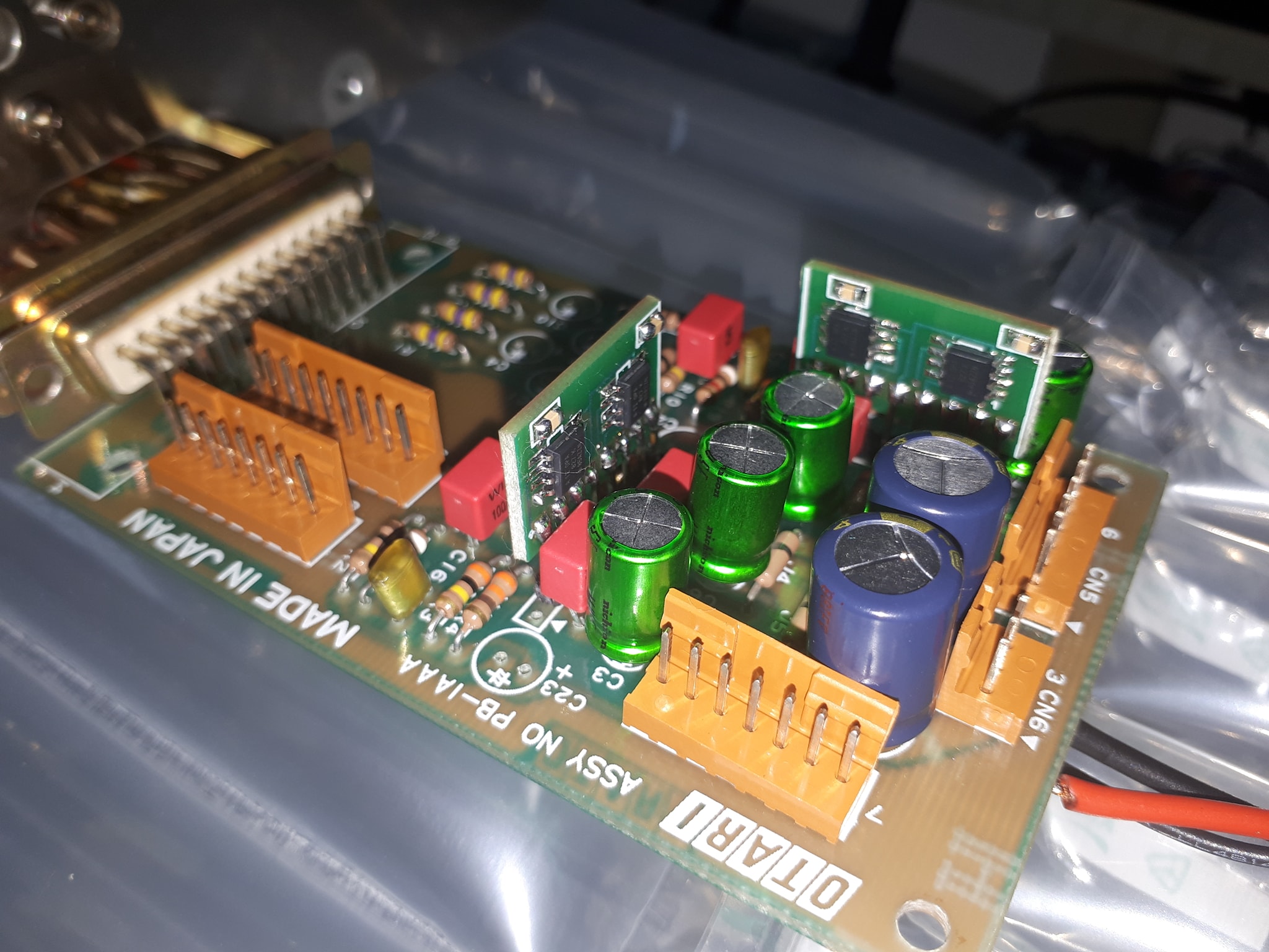
First lets focus to the important chains of the machine. The first one is the playback head pre-amplifier. Here are some photos of the original head pre-amplifier.
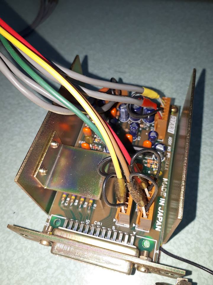
Now we are preparing for the replacement of the critical components of the board:
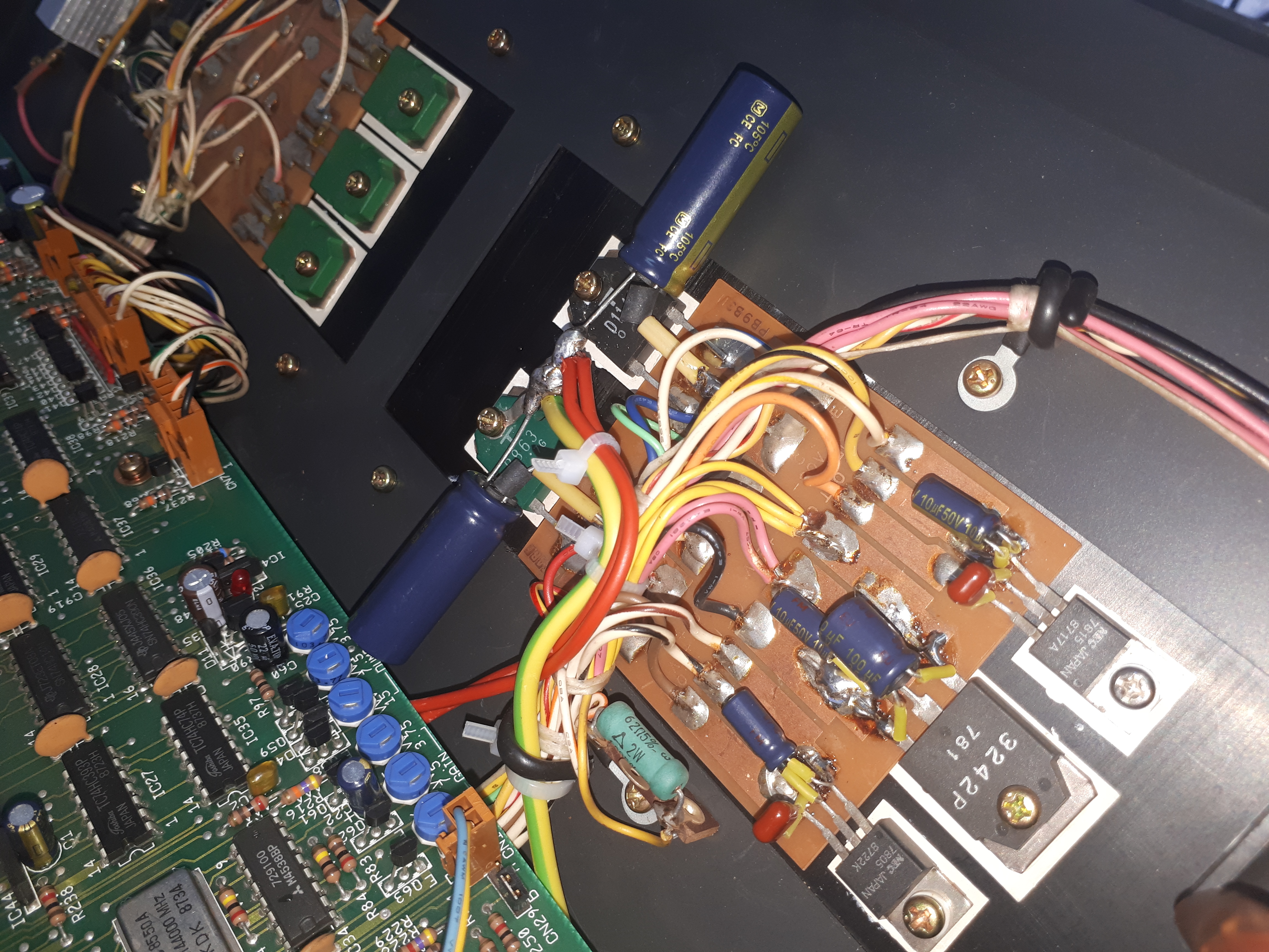
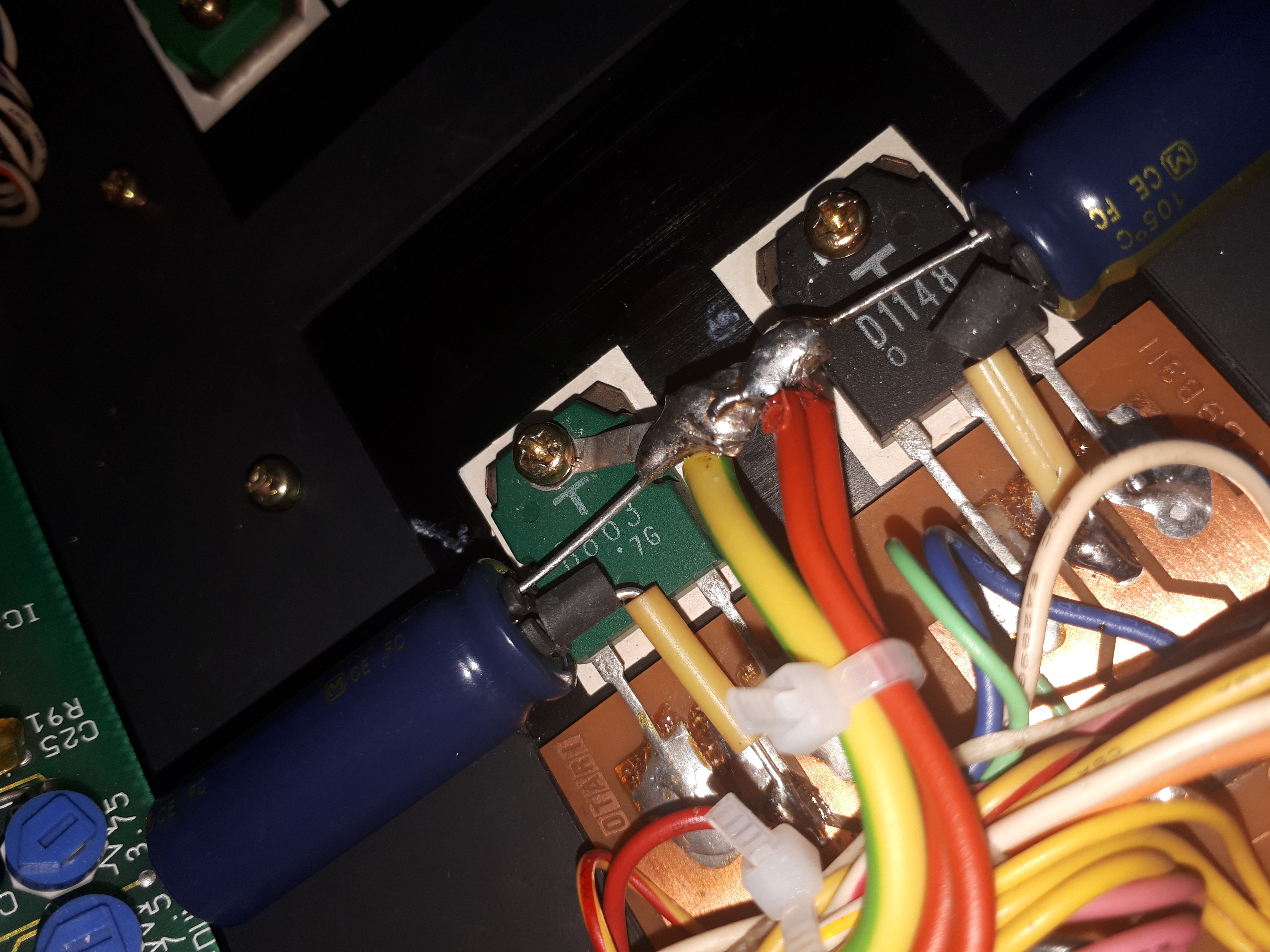
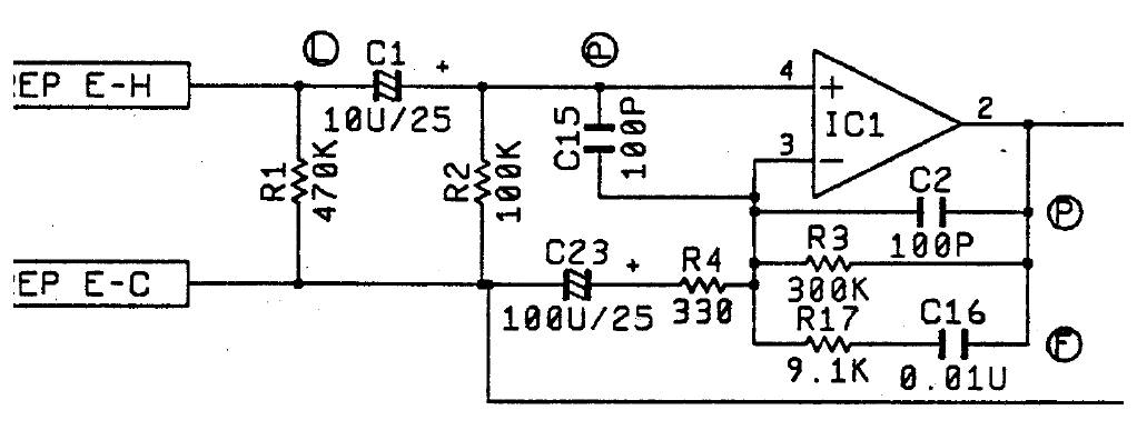 It is separated in its own metal shield box nearby the heads. The schematic use electrolytic coupling capacitors (C1 – the orange cylindrical ones) in the front of the heads, also the C23). They are very sensitive to interference comes from the power transformer and also the self noise of these capacitors is amplified by the higher gain of the preamp. They are locally shield by a metal plate but these capacitors tends to generate non-linear distortions and in the high performance machines the aim is to remove the first coupling capacitor. It is not easy task because of the common used BJT input op-amps that are used in the design. The BJT op-amp have significant DC input current that flows through the playback head and cause magnetization. That is why the simplest safe method is to use blocking capacitor in front of the head. The original op-amp was NJM2043 and its slew rate is too small (about 6V/uS). That is why we decide to replace it with OPA827. Its slew rate is about 28V/uS with a gain bandwidth of 22MHz. On the same time it is the lowest noise J-FET op-amp with voltage noise of 4nV/rtHz. The use of J-FET op-amp is mandatory to remove the DC bias current passing through playback head. That way we can simply short the C1 capacitors (for every channel) and completely remove them from the circuit. That mod improve the low-signal linearity and increase the S/N ratio. The OPA827 is precise balance op-amp and that fact can be used to remove and short the C23 capacitors from the circuit. These capacitors are used to set the DC offset at the output of the op-amp to be as close to zero. The OPA827 is good enough to supply better balancing so the use of C23 is not necessary after replacement of the op-amp. The goals from the mention mods:
- no input coupling capacitors (C1);
- no feedback resistor coupling capacitors (C23);
- improved low-frequency response;
- improved low signal distortion;
- improved signal-to-noise ratio;
- improved feedback response due to the fastest op-amp;
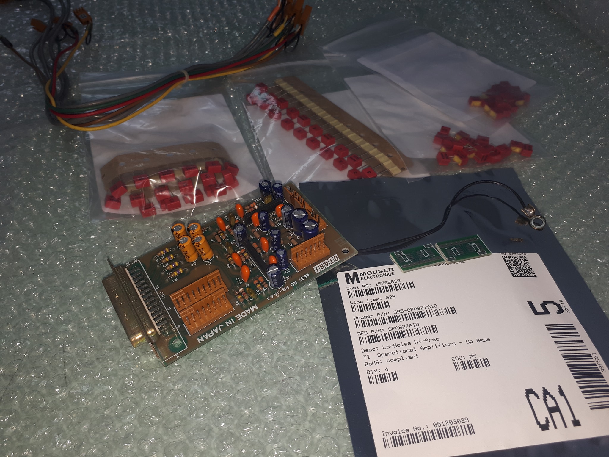
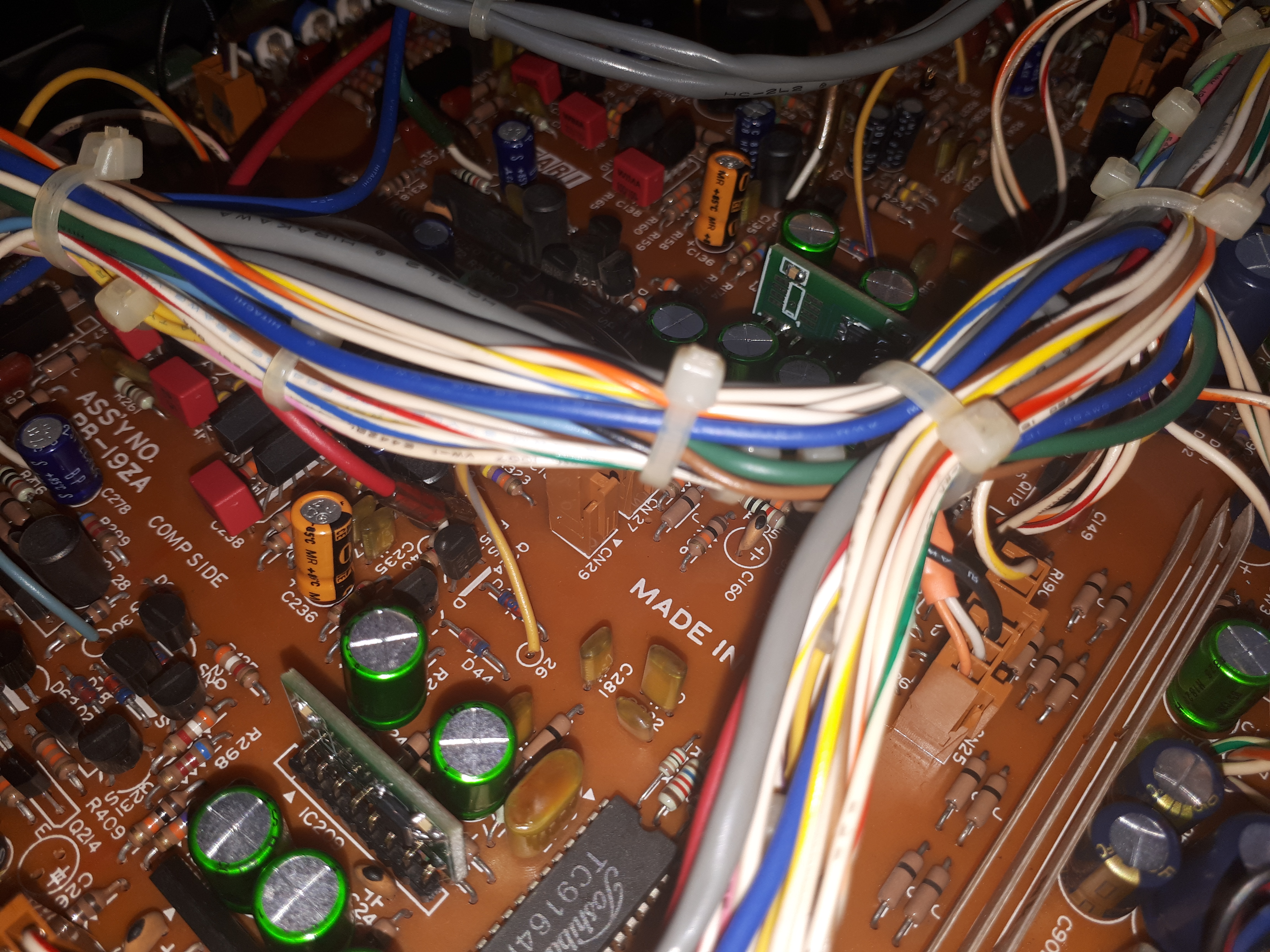
The main problem of op-amp replacement was that the OPA827 is only SMD version and also it is a single op-amp while the NJM2043 use SIP-9 footprint and is a dual op-amp. We develop a special socket to allow conversion between two SMD op-amps soldered to a small board to one SIP-8 socket. In fact the SIP-8 and SIP-9 pin versions are very close. On the 9-pin version the first pin is internally connected to the last pin9 and is connected to the positive power supply. The required mods to replace SIP9 with SIP8 socket is to left the PIN1 unconnected and to start with PIN2. On the PIN 2 we have to place the PIN1 of the SIP8 socket. That is all till one required attention! There are two integrated circuit into the board. The first one is powered by the PIN4 and PIN9 (the pin 1 of the SIP9 footprint is unused). The second one use pin 1 for the positive power supply but we left it unconnected when placed the new SIP-8 extension boards. It is required to solder a wire between the unconnected pin 1 and pin 9 at the bottom side of the board. Now everything is fine and we have to replace the power filter caps – we placed 470uF/25V (the blue Panasonic FC caps) and also re replaced the output coupling capacitors with bi-polar from the Muse series by Nichicon (33uF/16V). The measured DC offset the the op-amps was about 5mV which is close to zero and is good enough for the proper works of the design. Also we replace all the orange PP caps (100pF) with new WIMA film capacitors. The decision for the replacement of these capacitors is based on the “orange cap disease” which is noticed on most of the Nakamichi decks. These capacitors looks to be the same as the used orange caps by the Nakamichi. Here how it looks the test bench of the modified head amplifier:
The PB equalizer
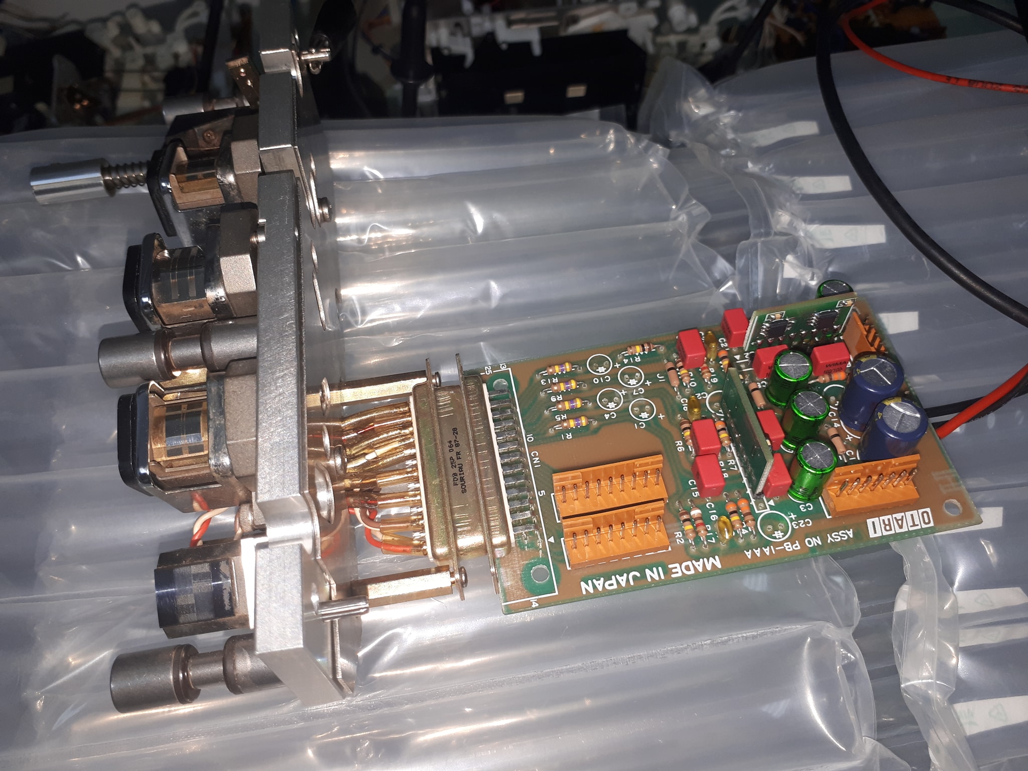
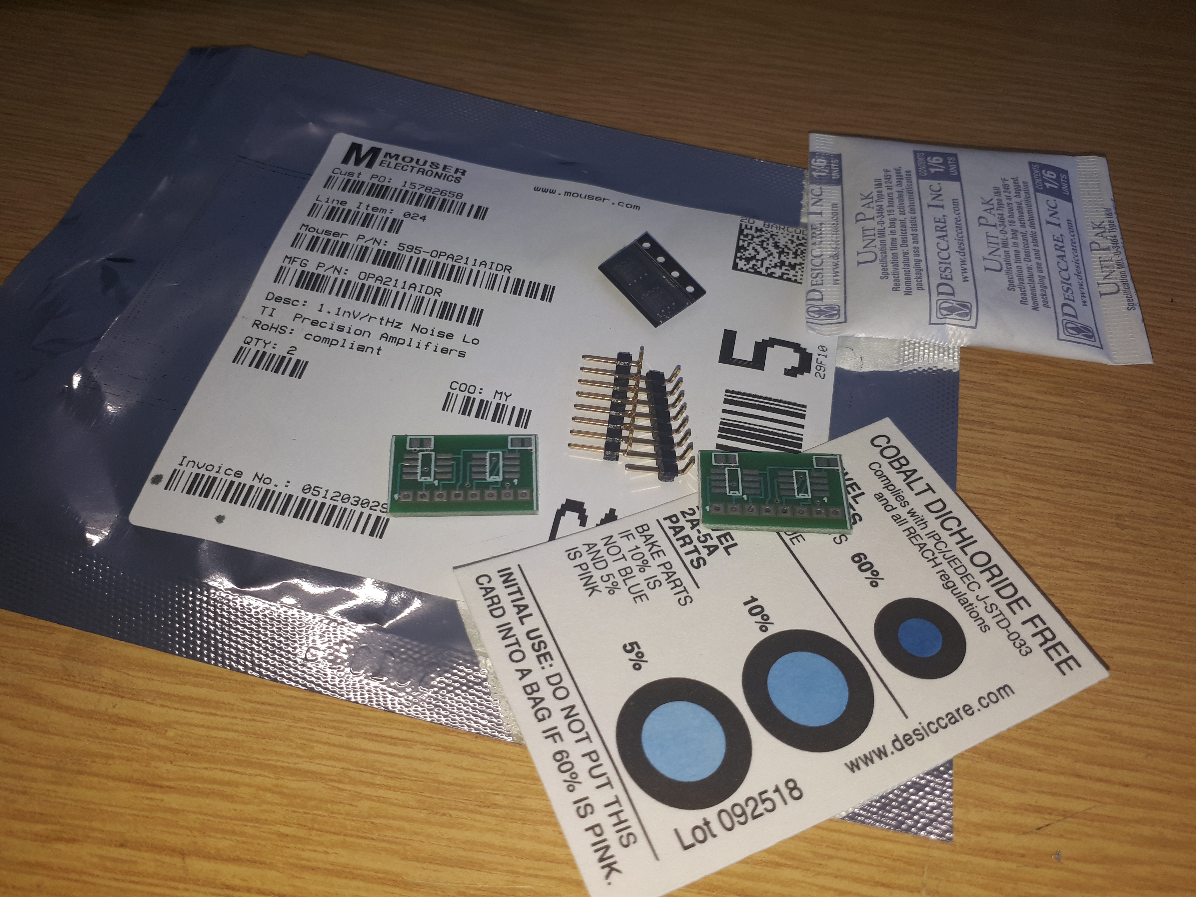
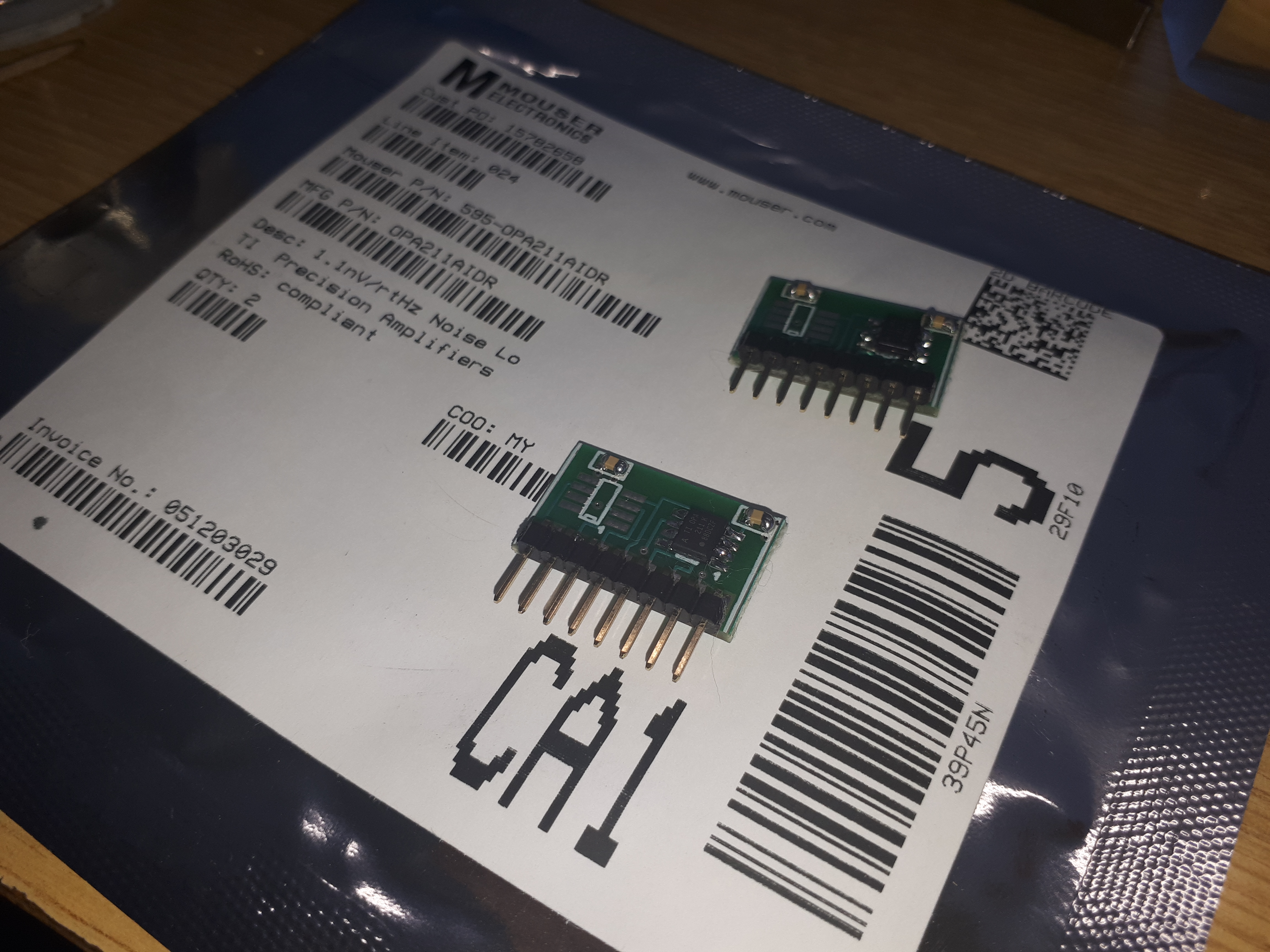
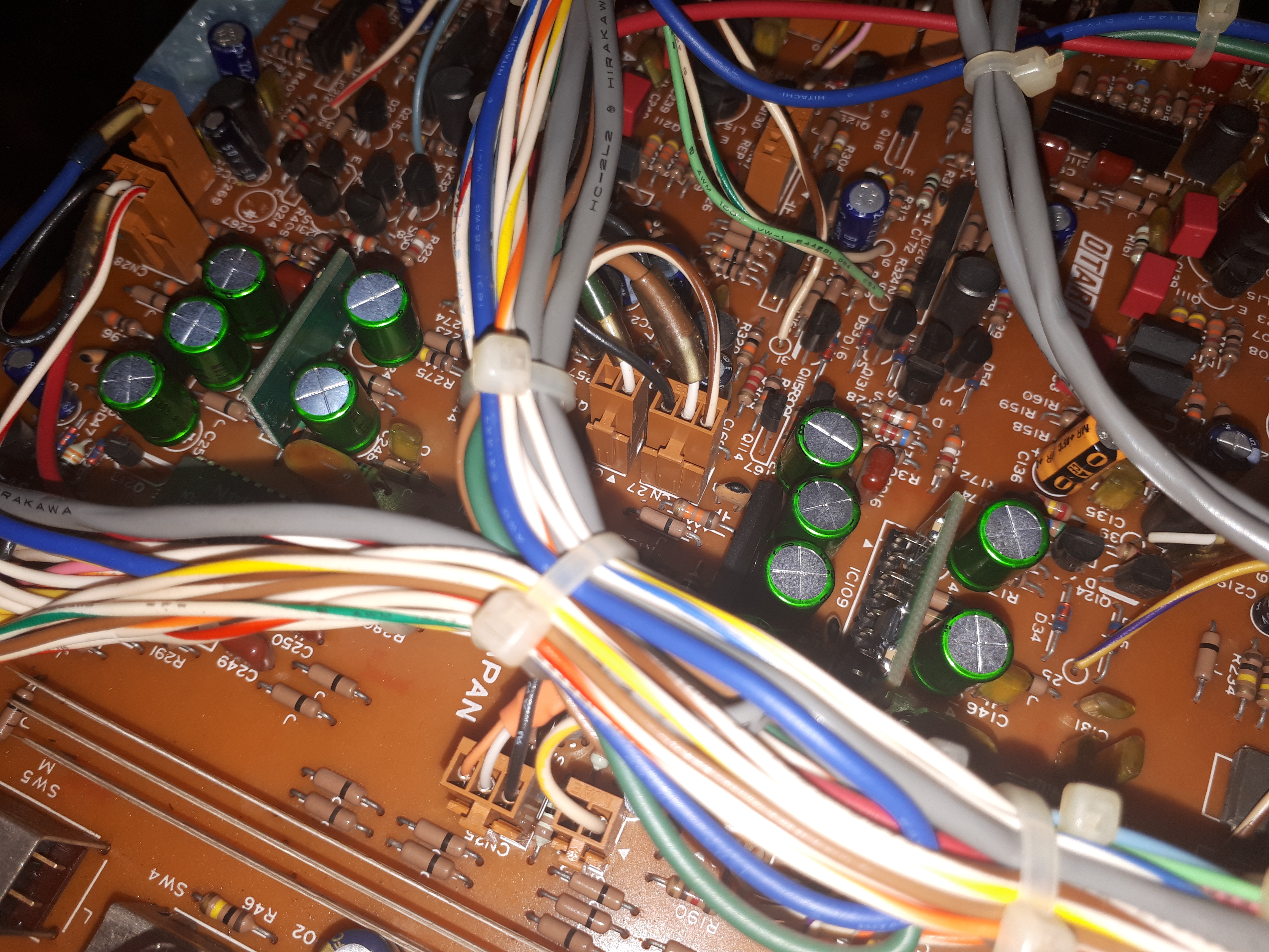
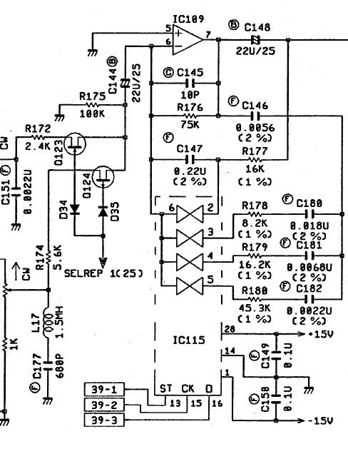 The signal is amplified and previously equalized by the head amplifier. Then it is passed to the head switch (repro/sync) and goes to the second fixed equalizer. In fact it is the main switchable equalizer that corrects the IEC/NAB frequency response for different speeds. The used op-amp there is M5219 which is not so bad at all. The equalization process require some LF and HF gain so we replaced the EQ op-amp (IC109) with the better one OPA211. OPA211 is one of the best sounding op-amps. Its input voltage noise is one of the lower ever made and is about 1.1nV/rtHz. The slew rate is about 27V/uS and the bandwidth is about 80MHz. Because the EQ board is based on inverting amplifier we decide to force on two criteria: low noise op-amp and at the same time the higher slew rate to improve the feedback response. The IC109 use traditional SIP-8 package. The OPA211 is single op-amp and is based on SMD SO-8 footprint. We need an extension board for the replacement. That is why we develop a custom made extension boards similar to the used ones in the head pre-amplifier. The IC109 requires only one channel – the second op-amp is not used in the design and is terminated. Its positive input is connected to the ground and the op-amp is used as follower. That is why we decided to completely remove the unused channel and to put only one OPA211 (the corresponding channel is IC209). Here are some photos of the replacement plus newer bi-polar capacitors (the green ones). We replace all the coupling bi-polar capacitors with Nichicon Muse and capacitance of 33uF instead of 22uF. That extends the low-frequency response of the machine.
XLR wiring
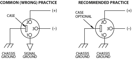 Several modifications were made on XLR balanced connectors. At the first look, the Otari use swapped ‘hot’ and ‘cold’ connections (pin 2 and pin3). It is fixed by swapping pin 2 and 3. But there exists still another urgent mistake! First lets comment the problems with the balanced lines in most pro equipment. Since standard XLR cables come with their shields tied to pin 1 at each end (the shells are not tied, nor need be), this means equipment using 3-pin, XLR-type connectors must tie pin 1 to the chassis (usually called chassis ground) — not the audio signal ground as is most common. Not using signal ground is the most radical departure from common pro-audio practice. Not that there is any argument about its validity. There isn’t. This is the right way to do it. So why doesn’t audio equipment come wired this way? Well, some does, and since 1993, more of it does. So why doesn’t everyone do it this way? Because life is messy, some things are hard to change, and there will always be equipment in use that was made before proper grounding practices were in effect.
The first thing is to choose the operation level between the HIGH/MID/LOW and the EU/US versions. Which one? The answer is not so easy and depends on the used tape and its over saturation ability. I always recommend to use IEC on 7 and 15ips using the MID reference level at 320nWb/m. Note that this is the EU recommendation. The US use 250nWb/m instead of 320nWb/m. For the NAB and 7ips I always recommend the LOW (250nWb/m). For some modern tapes it can be used the HIGH (510nWb/m).
Now we will comment the right way to measure the output voltage at the balanced line out connector. Most of the facts are described in another article but as a conclusion we will use the double of the measured voltage referred to ground (chassis) . As initial state we have to choose the output level between LOW or HIGH. The HIGH corresponds to 0 dBm while the LOW position of output level corresponds to -20 dBm. The machine is factory tuned for +4 dBm level, which is about 1.23V rms at 600 ohm load (the meaning dBm requires termination). The output driver of the MX55 use contemporary design using very low output impedance. That way it doesn’t matter the load impedance of the output. So we have to measure the half voltage at the hot and cold terminals of the XLR connector (pin 2 & 3), which is about 615 mV at zero dB on the meter.
The Grounding scheme
Now lets look at the original grounding circuit and the required grounding mods. It should use only one reference ground point. Otari MX55 follow this principle but in some strange way. In the good working designs the reference zero point is the connection of the main filter capacitors. MX55 use several voltage regulators – for the digital part and controls, for the audio chain, for the motor drivers, for the bottom audio board and for the XLR amplifier board. The ground of each voltages is connected together in the control board at the power supply section. All of the powers use couplings between the chains so this approach is not so good because the connection can increase the resistance of the net. How it is made the original grounding of the MX55: the zero reference point of the main filter capacitors goes to the connector 8 to the main Audio Amp PCA (connector 16, pin 3). The regulator transistors and the voltage regulator ICs are insulated from the chassis by plastic washers. That way they do not reflect to the grounding of the chassis – the chassis should be connected to the ground at one point. The point is the playback head amplifier ground. It is connected by 3 pin power cable to the ground of the main Audio Amp PCA (connector 6, pin 2 on the Head Amp board). That way the chassis is connected to the reference point of the filter caps passing the several couplings (2 for the Head Amp + 2 for the Audio Amp). The ground of the XLRs is connected to the Audio Amp PCA by the shield of the cables. As described in the previous section it is not the recommended grounding scheme. We changed the grounding as follows:
First we decide to ground the chassis directly at the reference point of main filter caps. We solder a short wire with wider diameter to the ground of the power section on the control board nearby the filter caps. That way we removed the problems with the coupling connections. The grounding wire comes nearby to the regulation transistor, where we place another two power filter capacitor after the voltage regulators for the audio chain. The reference zero point is the connection of these caps to the chassis. Because the backside chassis is connected by the main chassis on a flexible mechanical parts we decide to make another solid connection of the reference backside chassis to the front side chassis (the point where the HeadAmp is connected to the chassis).
Now we have good reference chassis ground. At the reference point of the capacitors that we used to connect the chassis now we place another wire which will connect the ground of the XLR connectors. That way we fully supply the recommendation as mention above. We cut the shield wire of the cables that connect the XLR connectors to the main Audio board (pin 1) to reduce grounding loops. We solder hard wire between the ground of the Audio Amp board and the reference zero point. The same was done for the HeadAmp board and for the balanced Output drivers. On the same time we cut the grounding wires on the relevant connectors to avoid grounding loops.
The Output buffer symmetry
Investigating the circuit we notice that the output amplitudes of the HOT (OUT 1H) and COLD (OUT 1C) pin on the output XLR connectors are not the same (refer to ground). The difference is not significant – the measured amplitude of 800mV on each pin has difference of several mV. The connection grounding scheme requires full balanced symmetry for canceling the grounding current. That is why we decided to make simple mod that can set precisely the gain for every H and C channel to match the output amplitude refer to ground.
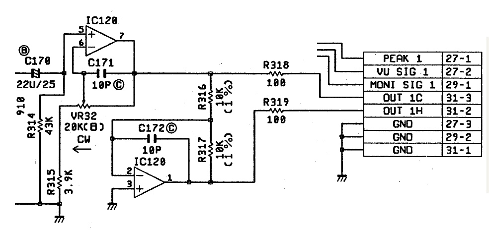
Here is the schematic of the phase rotation circuit for the output balanced driver. The balanced driver is a high power follower for the H and C signal. These signals have to be in opposite phase directions (180 degree). IC220 convert the normal unbalanced signal to balanced. The first part of the IC220 set the output gain via the VR32 for the COLD signal. The second part is inverting amplifier with gain of 1. To fix the symmetry of the output signal after the balanced driver we need to change the gain for one of the channels that way to compensate the differences of the driver chain. While the COLD (C) signal is fixed we decide to change the gain of the HOT (H) signal by adding a variable resistor. We cut the R317 connection and add in series a variable resistor with resistance of 2,2k. The value of R317 was replaced from 10k to 9,1k. Now we have ability to change the gain for the H line to match exactly the gain for the C line.
Reference levels & Alignment
It is important to press (activate) the SRL buttons and to set the volume on input and output knobs to zero. The first thing is to set the internal test generator level and the zero reading of the VU meters. The machine was designed that way we cannot tune the VU meters readings individually. We will implement simple mod to fix this problem. But at the first time we have to align the 1kHz test generator. We have to set the machine to monitor and to switch on the 1kHz generator by the generator mode switch. There are two variable resistors on the audio board – VR1 & VR2. We have to measure the distortion of the 1kHz signal (or to inspect the spectrum) and to set VR1 for minimum third harmonic distortion. The VR2 set the generator level (operating level) for the zero reading of the VU meters. We will notice a little difference between the CH1 and CH2. We have to change the values of R302 or R402 to match the readings on both VU meters. In our case we put in parallel to the R302 a 220k resistor. That compensate the gain of one of the monitoring channel.
Now we have good aligned reference test generator. At 0dB readings on the meters now we have to set the Output level of the XLR connectors using the VR23 for both channels. We chose the operating level at HIGH on +4dbm and expect to measure 1,23V between the hot and cold pins or 615mV on each pin refer to ground. No we have good alignment output driver.
Now we have to set the input level sensitivity with the VR11. We have to set 1.23V signal (1kHz) at the input pins of the Line IN (between hot and cold pins). Note that the signal have to be balanced. If the measurement are made with unbalanced signal the reading on the VU meter will be about -6dB. Now we have to switch off the test generator. The input signal appears at the output. We have to set the VR11 for CH1 and CH2 that way the VU meter reach 0dB. On the other hand more precisely we can use voltmeter and making a measurement of the input and output signal. We have to get the same readings for the output signal – in case we set 1,23V on the input XLR we will expect to get 1,23V on the output XLR. Now we have good alignment of the operating level.
The Peak level indicator
It follows the tuning of the peak meters. Originally the machine was set to activate the peak meters at 1040 nWb/m which is too high at all. The choice of the peak level depends on tape you use. Maybe it is good choice is using with tapes like SM900 (MOL at 1kHz is +14dB). Here it is some comparison of the MOL level for the contemporary tapes:
- SM900 – operating level for 15 and 30 ips (IEC) is 320 nWb/m and MOL is +14db;
- SM911 – operating level for 15 and 30 ips (IEC) is 320 nWb/m and MOL is +13db;
- SM468 (high bias) – operating level for 15 and 30 ips (IEC) is 320 nWb/m and MOL is +12db;
- LPR90 (long play version of SM900) – operating level for 15 ips is 320 nWb/m and MOL is +10db;
- LPR35 (long play version of SM911)- operating level for 15 and 7,5 ips (IEC) is 320 nWb/m and MOL is +7,5db;
We plan to use the machine with LPR35 and that is why we will set the peak indicator for the MOL (Maximum Output Level) at 3% THD, which is 7.5dB higher than the reference operating level of 320 nWb/m. That is why we put 1kHz signal at the output level of 7.5dB higher than the reference (2.92V equivalent to 760nWb/m) and set the VR1 on the backside of the VU meters placed on the output drivers board that way the peak leds start illuminate.
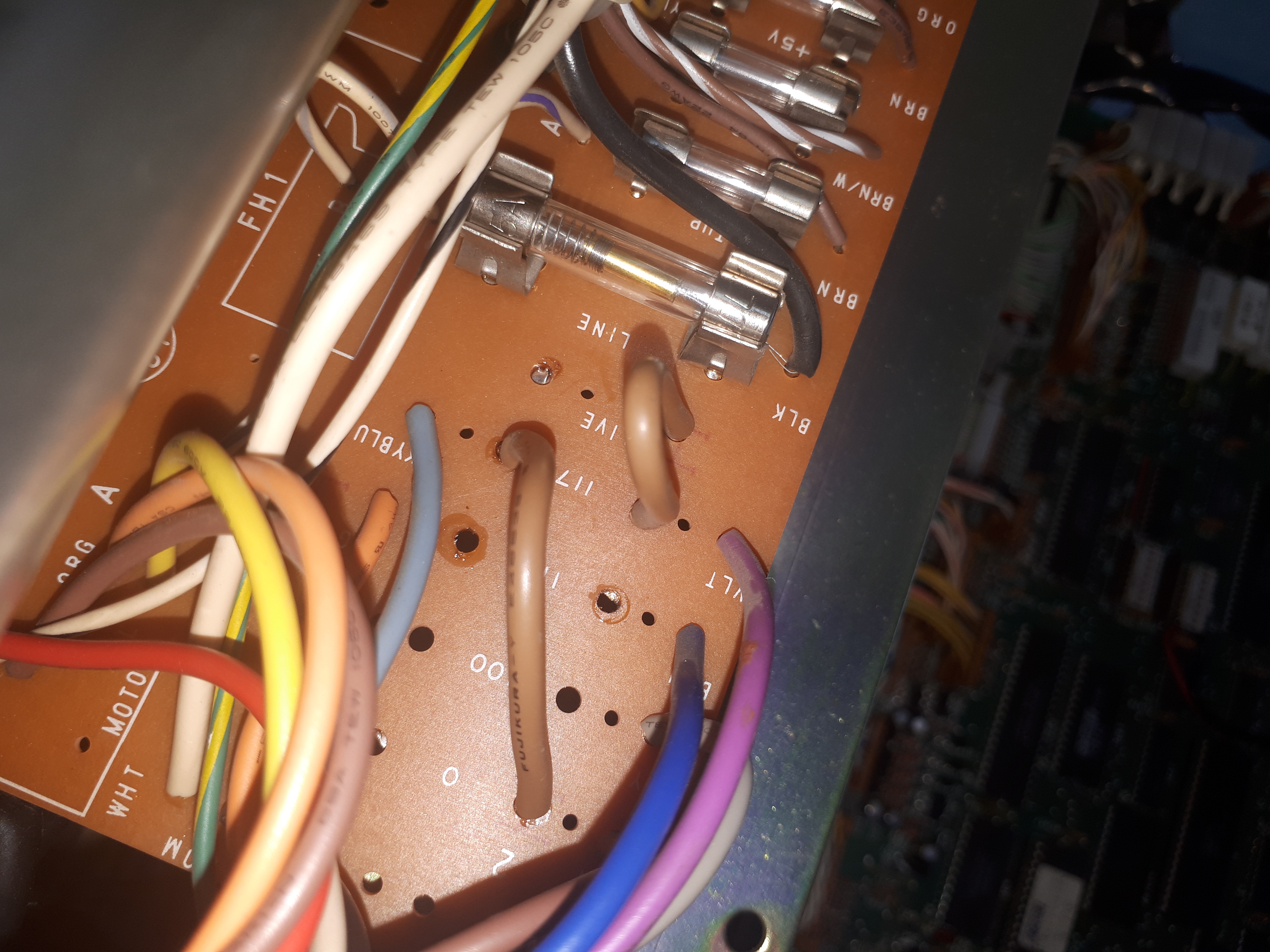
Setting the machine for ~240V
Since modern standard for the power line in EU moved from 220V to 230V the standard power position for the 220V increase the flux into the power transformer. This increase the hum interference into the heads and the heat power loss. We switched the machine for 240V which covers the standard +/-10% power rating and also optimise the flux and head loss into the power transformer. The photo shows how the two brown jumper wires need to be placed for the 240V power setting.
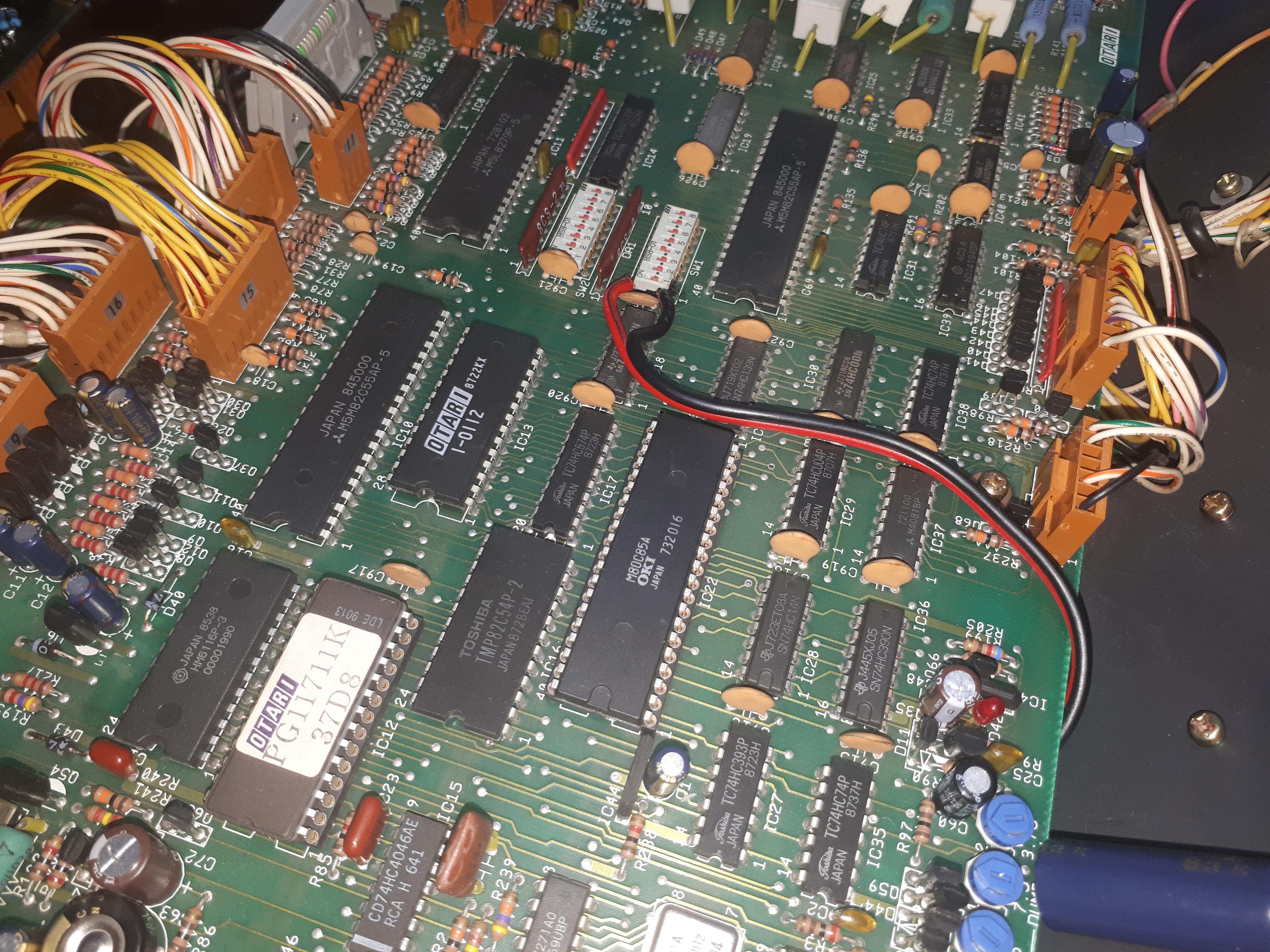
The High/Low speed external switch
We placed external speed switch at the bottom panel of the machine. Since the machine is two speed based it can handle bot four speed by internally switching. To switch the machine for low speed you need to short the first jumper on the SW1 (the soldered wires at the pins of the jumper on the photo). Now the machine can work both on 3,75 & 7,5 ips or at 7,5 and 15 ips. The high speed front panel switch then can vary for 30 ips monitoring or for 15 ips monitoring.
The Capstan control and Alignment
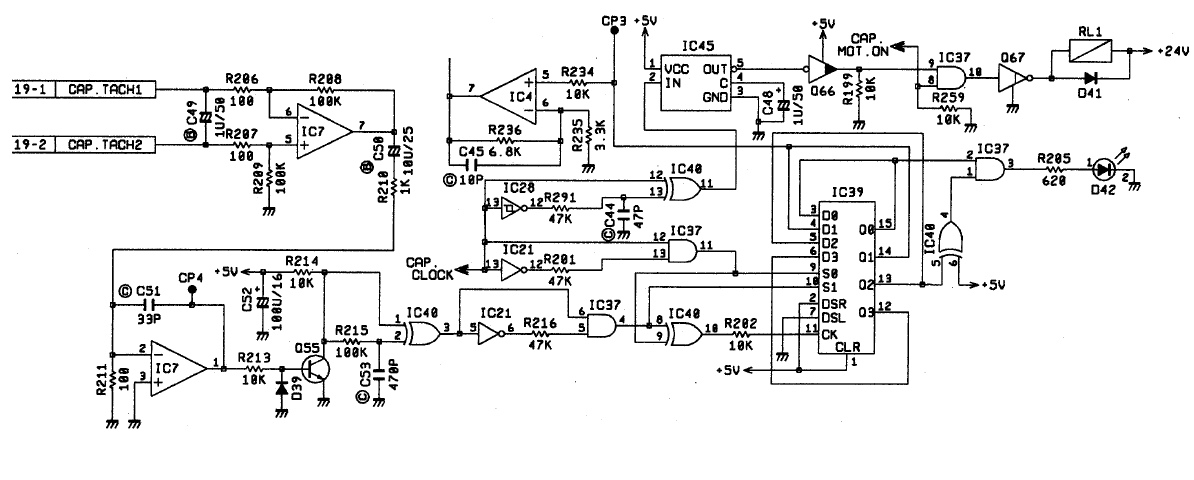 The capstan motor control is based on reference quartz frequency comparison. The control loop is made using shift registers. The 3 bit shift register is filled by zeros (0) from one of the direction and by ones (1) at the opposite direction. The clock of the shift registers is controlled by the reference crystal clock and the direction is controlled by the tacho generator clock, which measure the real speed of the capstan motor. This similar approach is used in the Revox B710 and B215 machines. If the speed is correct then a short clock pulses with zero meanings comes to the shift register mode pins (S0 and S1). In this mode the output state of the shift register is saved to the registers – it means there is no speed or control change of the current state of the control loop. If the controlled frequency is lower or higher then follows switching of the shift register direction. At the middle output of the shift registers goes a high or low signal depends on the speed error. This signal is integrated and filtered by analogue filter. At the middle output of the shift register is connected the control test point CP3 (pin 14) that we will use for the alignment process of the capstan motor. We have to measure a 50% duty cycle on normal tape movement for all of the speed modes. What we have to do: first set the machine at 15 ips, load a tape, set the jumper CN29 to A position, play the tape and tune the VR9 that way you have a 50% duty cycle on the CP3. Then move the jumper CN29 to B position and now tune the VR6 playing the tape that way you reach 50% duty cycle on CP3. Switch the machine to 7,5 ips and tune the VR5 for 50% duty cycle while still playing the tape. Then switch the machine to 3,75 ips and tune the VR4 for 50% duty cycle while still playing the tape. Now you have to set the release time of the filter loop by tune the VR1, VR2 and VR3 for the 3 different speeds. When you put mechanical tension to the capstan motor you have to observe the duty cycle on the CP3 and set the VR1-3 for the fastest response to normal state. If you cannot do that just set the VR1-3 to the middle position and this setting is fine at all. Now you have good aligned capstan motor control loop.
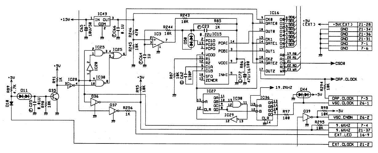
It is interesting how the quartz reference clock is done in the MX55. The reference clock is named as CAP. CLOCK. It is generated by another complex circuit and that approach is due the pitch control which can vary the tape speed and this pitch control is also quartz stabilised. The CAP CLOCK is generated by 4046 PLL circuit. The PLL is implemented by 3 software controlled dividers (IC16). The main oscillator clock is previously divide by fixed divider and forms 19.2kHz reference clock which goes to pin 15 of IC36. It is divided by two and forms the reference input clock for the PLL of 9.6kHz. The VCO divider, the input divider and the output divider are formed by software controlled counter (IC16) which consist of 2 16-bit counters. Every counter can be addressed individually and set as binary or decimal. The IC16 is TMP82C54P-2 which can supply different programmable modes for the internal 3 timers – increment or decrement modes, auto load mode etc. All the 3 timers allow the PLL to generate wide reference frequencies at its output. The MX55 have one another working mode with external clock. In this mode the reference clock is feed by the Q35 and bypass the reference 9.6kHz clock.
Recording equalisation
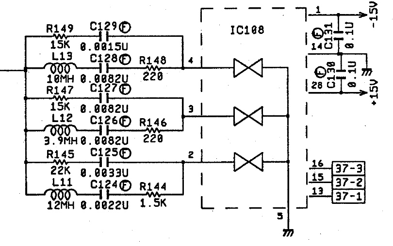 The last thing into the restoration project was to align the recording high frequency LC circuit to mach precisely the flat frequency response. When we try to align with the standard settings of the REC EQ trim pot and BIAS we can touch a good almost flat recording frequency response on the LPR35 tapes. There is a roll-off starting at 16kHz and at the 21kHz the roll-off is about -2dB. We want to make extremely flat frequency response up tp 23kHz so we made a mods into the LC circuit for the head loss compensation for the 15ips (L11) and for the 7.5ips (L12). We changed the values of the resonance capacitors and of the serial resistors into the resonance circuits. The standard serial resistors (R146, R144) were 220ohm and we replaced them with 33R resistors. We changed the resonance capacitors by adding in parallel additional small ones – 820pF in parallel to C124 for the L11 tank and 1.5nF in parallel to C126 for the L12 tank (for both channels).
In a conclusion…
…the machine got very pleasant sounding and extremely flat recording. The work of the restoration project was complex and hard and took about full 5 working days. The labour cost for that kind of work is usually about 1200 euro. The new 2.75mm half track heads set (PB and REC) was about 500 euro, the Athan pinch roller was about $110 including the shipping, the cost for new breaks and new EE SKF bearings was about 70 euro. The cost for the electronic components – capacitors, op-amps and extension boards was about 312 euro. The noise of the new EE bearings from SKF are higher but it needs a lot of time to get into normal working parameters. The total price for the project is not so cheap but we have a completely new machine. If we take into account the price of the MX55 machine the final cost is much lower than the new R2R projects like Ballfinger (about 25k euro) or Thorens (only PB for 12k euro).