Introduction
The Dragon model made by Nakamichi is one of the top cassette decks and it is unique with its playback auto azimuth correction system which improves the high frequency loss due to the azimuth errors in the records. In the past several years we serviced around 10 machines and made full rebuild of 4 of them and that is why we decide to describe the construction of the machine at the same time we will describe the required modifications for improvements of the sound quality. The machine was manufactured in the early 1982 but it was manufactured up to the 1995. The serial numbers of 30’100 were manufactured about 1993 and that fact can be seen on the mark on the flywheels. The early serial numbers up to 1’000 were full of issues and they were fixed on the fly by fabric patch on the mainboard:
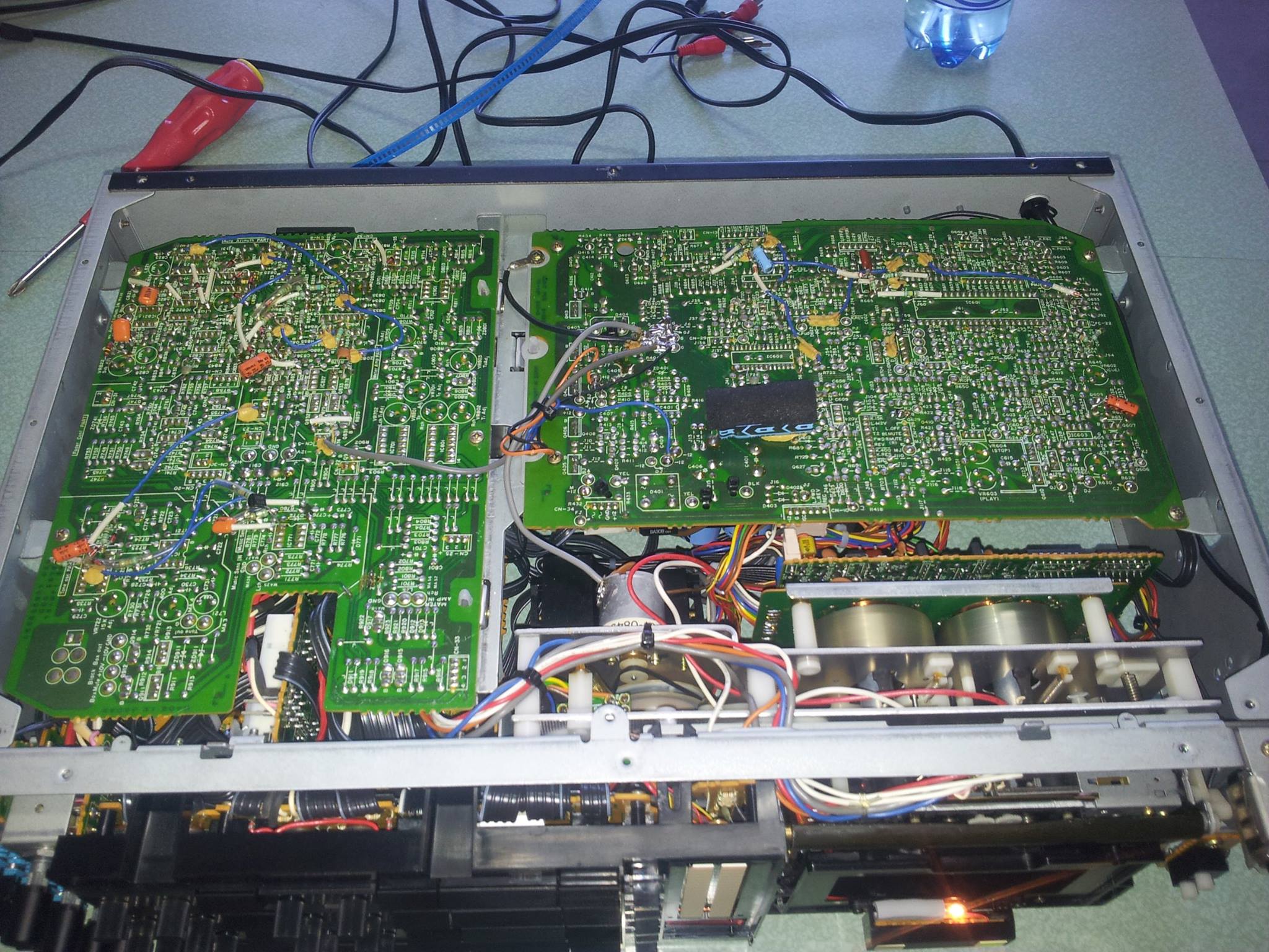
The late serial numbers use external Dolby module outside the mainboard. The Dolby chains on the mainboard were removed and it was a strange decision. Maybe the cost of the early Dolby chips was the reason for this decision. The external Dolby module is 2 channel and use only two Sony chips instead of the four TEA0652 chips. Also the Sony chip has build in spectral skewing circuit without coils. The traditional Dolby module use four 36mH coils, which are also high cost components. The coil replacement in the Sony chip is made by electrically simulation of inductance and is more precise because the coils high tolerance. Never mind on the serial number the machines are made using polar Nichicon capacitors. For me it is bad idea and increase the distortions. Nakamichi used these polar capacitors in opposite connections to simulate bipolar capacitors and that approach significantly reduce the distortions but the signal path is full of coupling electrolytic capacitors. The used op-amps are made by JRC and the precise low noise are J-FET based on NJM-072D. It is not bad at all but for now there a lot of better replacements. The rebuilds made in the lab are based on some primary major steps:
- replacement of all the orange caps with new polypropylene ones;
- replacement of all the electrolytic caps with new ones based on Elna Silmic II, Panasonic FC and Nichicon Muse (bipolar);
- rebuild of the mechanism – replacement of the idler and belts and new lubrication of the parts;
Some photos can be seen at the official Facebook page of the lab.
The mods & description
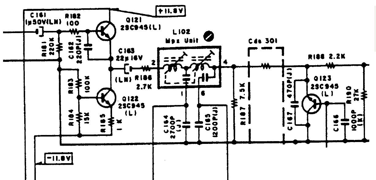
Now lets comment the modifications by chains and the explanation why they are required. Starting with the line input buffer we can notice one electrolytic capacitor in the front of the buffer. It was bad idea at all but it was required by the bipolar input design of the buffer. It is also well self polarized by the input bias of the Q121 (about -0.7V on voltage drop on the R181). The typical signal amplitudes on the base are about ~35mV at 0dB, so the polarization voltage is enough to drive to reduce the distortions of the C161 and C163. The voltage at the output of the buffer is about -1.5V referred to the ground. That is the polarization voltage of the output coupling capacitor of the buffer. The higher noise current of the front top transistor generate significant noise component when the inputs a left open and the volume control knobs are set to maximum. The measured rms noise voltage at the line output was about 0,35mV on the monitor position with open input and volume knobs set to max. The second major problem with the input buffer is its own transition frequency response. Looking at the output of the buffer we will notice the MPX filter, which can be enabled by grounding its terminals (lines goes down by the MPX coil). When this filter is disabled its cut off frequency goes higher but still it is low-pass filter. It is a good approach at all to eliminate the unused spectrum content at the input of the machine. The measurement confirm about -1.2dB for the 21kHz compared to the 400Hz. That is why we decide to correct the transition frequency response to linear by put a 3.3k resistor in parallel to R186. That fixed the liear transition frequency on 22kHz. Now we decide to replace the top transistor of the buffer with low noise J-FET and to eliminate the input electrolytic capacitor. We placed a 2SK170BL and shorted the C161. The bias current of the buffer was set to 0.7mA, which is good enough for the buffer to work in pure class A. The output voltage of the buffer now was +0.7V referred to ground (instead of -1.5V). That is why the polarity of the C163 needs to be reversed. We set a 22uF Elna Silmic II capacitor in parallel with 10nF film PP cap for the C163 – the plus terminal goes to the source terminal of the 2SK170. Now the measured self noise of the line-out of the machine goes to 0,25mV rms (instead of 0,35mV). The filter power caps of the buffer were oversize to 1’000uF/16V. The default value was too small (100uF). Now we have a good working buffer and one major improvement – absence of the input coupling electrolytic capacitor, which is sensitive to distortion, noise and interference in the input high impedance!
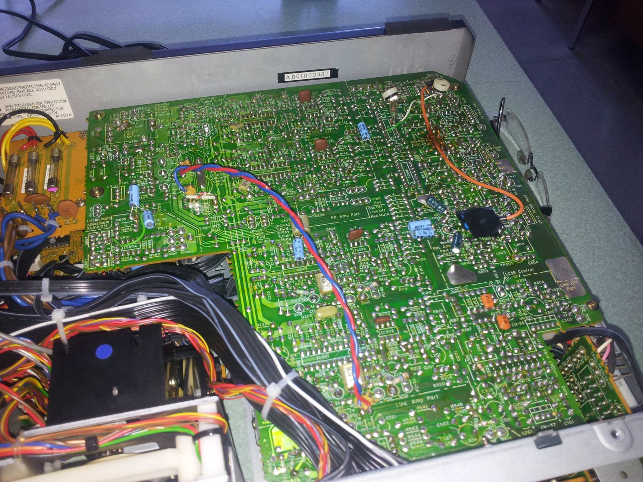
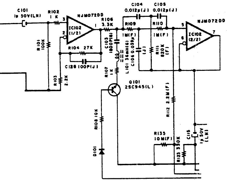 The output of the MXP filter goes directly to optically controlled volume (CDS301) for auto fade function. There are no coupling capacitors. The volume control is based on variable photo resistor which is driven by a optically by one led diode for both channels. Then the out of the photo resistor is connected to the input of the main line in preamplifier. The input signal of about 30mV is amplified to 387.5mV (which is the system Dolby level). Nakamichi use J-FET input op-amp for IC102 (NJM072D). The circuit specify one coupling capacitor (C101) but in the board it is shorted by a jumper connection. So the only one existing coupling capacitor is at the output of the subsonic filter (second part of IC102). It is connected to the pin 7 of IC102 and the second terminal of the capacitor goes directly to the monitor (tape/source) switch. The capacitor is grounded by R123 to set its zero potential for the monitor switch. The measured DC offset of pin 7 is about 33mV. We replaced the IC102 with contemporary good sounding OPA2140 rail-to-rail op-amp. Then the DC offset was reduced significantly to 0.3mV. That is why we placed bipolar coupling capacitor for C115. At the same time pin 7 drives directly the input of the Dolby chip. Every DC offset can cause the incorrect work of the Dolby processor. The DC offset was fixed by the good precision of the OPA2140 op-amp. If look at the subsonic filter we will notice the high resistance values of 1M and 820k. These resistors require a JFET based op-amp to reduce the additional current noise component caused by the higher value of the resistors. That is why we based the OPA2140 – it is a dual op-amp with relative low voltage noise of 5.1nV/rtHz and high slew rate (20V/uS).
Switching on the subsonic filter is done by a switch, which short cuts the R134 (10M). Then the R112 (2.2M) takes a part of the filter instead the summing resistance of 12,2M. Another electrical switch Q101 takes a part of the control of Dolby C spectral skewing circuit. Traditionally this circuit is a part of the Dolby chip but Nakamichi decided to put it outside the Dolby module. The input circuit is placed in the front of the subsonic filter, while the output one is placed after the decoding Dolby module (in the output buffer amp). The first part of IC102 acts not only as a amplifier but also as impedance converter between the MPX filer and the Dolby C spectral skewing circuit. The MPX filter requires high input impedance, while the spectral skewing circuit requires low output impedance of the driver.
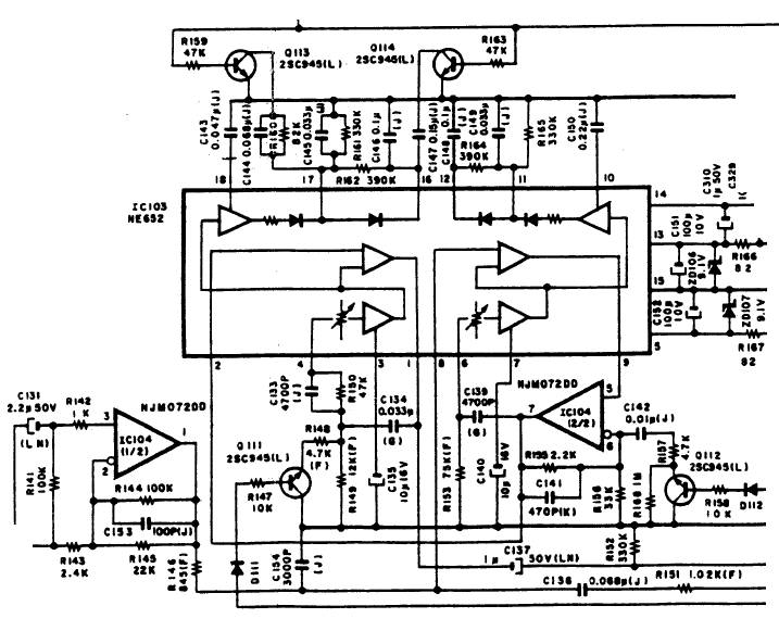 The improvement of Dolby modules is based on replacement of the orange caps and also the oversize of the power filter capacitors. Every chip has its own regulated supply by two zener diodes and filtered by two electrolytic capacitors. The default value of the filter capacitors is 100uF/10V. We replace these capacitors by 1’000uF/10V. At the playback Dolby chip there are two op-amps (build in one dual chip). The used one was the JFET NJM072D. The offset at the output of playback Dolby module was about 60mV so we decide to replace the op-amps again with the JFET OPA2140. The DC offset after replacement was reduced to 2mV. The input coupling capacitor (C131) and the output coupling capacitor (C137) were replaced with bipolar. Now lets comment the improvement of the playback frequency response. The original frequency response is well balanced and is flat measured with the Teac MTT256 test tape. However there is a roll off at 4kHz with a 1.8dB and the starting point is about 500Hz. It is not a significant problem but we decide to fix it with a simple mod: putting a series RC network (4.7nF + 20k) in parallel to the R143 solve this problem. The network increase the gain of the op-amp starting at about 500Hz up to the 4kHz and the increase is about 1dB. It does not require complementary compensation at the recording chain – the bias correction still can supply the flat recording frequency response.
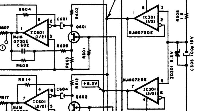 The playback amplifier of the Dragon use similar to BX300 topology. It uses front J-FET external transistor and current feedback for the equalization circuit. The reference power supply for the front transistors is made by a voltage follower and is stabilized by external zener diode and filter capacitor. Because the relative low signal levels and the importance of the lowest noise components in the front stage we replace the IC301, which is the power source for the first transistor with no compromise AD797. AD797 is the possible lowest voltage noise BJT op-amp and it is better for use only for the low input impedance sources because of its relative higher input current noise. The voltage noise of the default NJM072D is about 8nV/rtHz and appears directly to the load resistor of the first transistor. Every channel (there are 6 channels) consume about 1mA from the output of the IC301. AD797 can supply up to 50mA on its output. The voltage noise of AD797 is about 0.95nV/rtHz. Additional noise component will be produced by the higher noise current (2.7pA/rtHz) passed by the source resistance. The source impedance of the input is formed by the zener diode ZD301 in parallel to the pull-up resistor R301 and the filter capacitor C305. We replace the C305 with oversize Panasonic FC capacitor of 820uF/16V. The resultant source impedance is very close to zero so it not produces additional noise component at the output. We place another one protection diode in parallel to R301 (cathode connects to the +20V line).
The AD797 is good for reference voltage source but at unity gain (work as follower) it oscillates. The oscillation frequency is about 40MHz and the measured amplitude is about 1-2mV. It is not so high but in out design it is critical. The Analog Devices offers a circuit with one serial resistor to the inverting input. The inverting input is not connected directly to the output and this prevents the op-amp from oscillation. The serial resistor increase the self noise of about 2nV/rtHz – that is stupid idea because the advantage we want to use is the lower output noise. We decide to try another method to improve the stability of the op-amp. Using a Zobel network at the output of the op-amp fix the problem with the oscillations. We placed in a serial connection (33R resistor and 100nF capacitor) to the output of the AD797. The first terminal of the Zobel network (33R resistor) was connected to the op-amp output, while the terminal of the capacitor was connected to the ground. Now we have a stable work with no oscillation, a high slew rate and very low noise (0.95nV/rtHz) for the power supply of the first amplification transistors.
Now it was time to choose good replacement of the IC601. It is very sensitive to the noise performance of the entire playback amplifier. We decide to choose no compromise OPA827, which is J-FET op-amp with high slew rate about 28V/uS and voltage noise of 4nV/rtHz. OPA827 is not dual op-amp that is why we used special small extension boards for soldering two single SMD op-ams to one dual DIP extension.
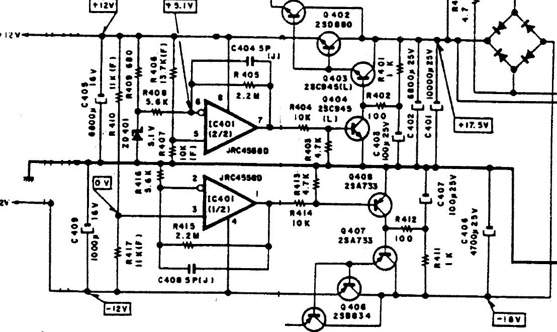 Most of the work of the op-amps replacement was done but still there are several important op-amps in the machine. The first one is the power supply regulator op-amp. In most designs the power supply regulators are not so important and often used regulators are based on LM8712 and LM7912. These are very noisy regulators and produces a lot of noise ripple at their outputs. Nakamichi used well designed regulator circuit that produces +12V supply and mirrors the negative voltage refer to its positive value. The regulator use dual op-amp in the control loop. For that kind of regulators it is important to use as fast as possible op-amps and on the other hand the lower noise of the op-amps is also mandatory. Every noise produced from the input stage of the regulator op-amp appear at the output of the power supply amplifier by the gain of the control loop. That is why we decide to replace the default JRC4558D with precise OPA2211 alternative. OPA2211 is dual version of the OPA211 and it voltage noise is about 1,1nV/rtHz, it is very fast and its slew rate is about 27V/uS and its bandwidth is around 80MHz. The input current noise of the OPA2211 is not so higher compared to the AD797 and is about 1.7pA/rtHz. It is not enough to change the op-amp in the power supply. The capacitors C403 and C407 were increased to 220uF/25V and that reduce the ripple in the base of the regulation transistors. It is good to make mods reducing some thermal noise caused by the resistance of several components. First we add additional electrolytic capacitor (100uF/16V) in parallel to the zener diode ZD401. The zener diodes are the components that generates significant noise and their self noise can be shorted by adding a capacitor in parallel otherwise this noise will be amplified by the gain of the control loop in the op-amp. The same with several resistors in the design: R417 and R406 – we placed in parallel capacitors (10uF/35V) to reduce their self thermal noise also to reduce the source impedance of the inputs of the op-amps which also reduce the generated noise component by the op-amp input current noise. The additional capacitors require protection diodes in parallel to the discharge resistors (the cathode need to be oriented to the positive polarity of the R409). One bypass capacitor of 100nF was soldered directly to the power supply pins of the op-amp (U401). Now the power supply is not better as the reference Walt Jung super regulator but is good enough.
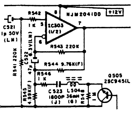 The next important chain is the line output buffer. The default op-amp is based on low offset NJM2041DD. Its bandwidth is only 7MHz – slew rate about 3V/uS. Nakamichi decided to remove the output coupling capacitor at the line-out terminal of the deck. This approach guarantee low distortions at the output – the distortions are caused by the coupling capacitor at the output at higher output current. The line out amp have to guarantee impedance conversion so a low impedance input can be connected to the output of the deck. In this case a high current will flow to the coupling capacitor that will cause significant distortions producing bad sounding. The problem with the absence of coupling capacitor is the zero DC stability of the output. That is why another electrolytic capacitor (C522) add to the design. This capacitor guarantees the same input impedance for both op-amp input for the DC (220k). And if the op-amp is well balanced that will produce zero offset at its output. The additional electrolytic coupling capacitor (C522 and C521) is a compromise and is not a good idea at all. The current flow through is not so high and produces low distortions. Still it is better to remove these caps from the signal path but this will produce significant DC offset at the line out. The first thing we do is to replace the output op-amp with LME49720. The new op-amp is very fast (20V/uS) and wide range (55MHz). It can easy drive 600 ohm load impedance. That is why we reduce the serial output resistor from 2.2k to 600 ohm. That will improve the output impedance of the machine and the line out can easy drive wide range of interconnection cables. Also the 600 ohm output impedance is a standard for most pro-audio equipment. The benefits of 600 ohm is that it can be connected directly to the input of measurement A-weighted noise filter for signal-to-noise measurements. The LME49720 is also a low-noise op-amp. Its self voltage noise is about 2.7nV/rtHz. When the new op-amp was soldered as a direct replacement its DC offset at the output was lower than 2mV, which is good enough (the output of the Dragon drives the audio signal at 1V amplitude). Now we test to remove the previous mention C521 and C522. We short cut these capacitors and notice very good output DC offset. The offset now is about 1,6mV which is also very good final result. Now the only coupling capacitor is the one at the output of the Dolby chips and it is bipolar bypassed by film capacitor.
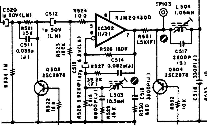 Finally we will review the most important part for the recording chain – the recording amplifier. The default op-amp is NJM2043 and is the noise improved version of NJM2041. Still the design is identical to the line-out buffer. There is one additional capacitor (C513), which improves the DC offset at the output. The record head is directly connected to the output of the recording amplifier without any DC coupling capacitor. For the recording every DC offset to the record head will produce additional noise on the records. That is why the easiest way is to use coupling capacitor with relative high capacitance (approach used in many pro and studio reel-to-reel recorders). The current flow to the recording head is significant and it produce high distortions in the coupling capacitor. That is why the best approach is to remove that capacitor but at the same time we have to guarantee true zero DC offset. That is why we will not remove the improvement offset capacitors in the recording chain (C520, C512 and C513). We changed these capacitors with bipolar from Nichicon for better performance. Now the question is about good replacement of the recording op-amp. The importance here is for low input noise and at the same time very low output offset. There are several potential but probably the best solution is to choose some laser trimmed op-amps. The OPA2227 and OPA2228 are good pretenders for low DC offset at the same time they are very low noise op-amps. Their input voltage noise is about 3nV/rtHz and at the same time the self noise current from the inputs is probably the best compared to the other BJT op-amps (about 0.4pA/rtHz). That is important fact because most of the additional equalization components in the recording circuit have relatively high impedance. We decide to use the OPA2227 due its improved stability compared to the OPA2228. Now the measured DC offset at the output of the recording amplifier is lower than 0.4mV. The original offset of the circuit was about 8-10mV which is not bad at all – due to the additional serial resistance (which makes the recording amplifier to be equivalent of current source) the DC current that flows to the recording head is low enough. The DC current was improved at least 20 times or more. Now the dominant factor for the noise in the recording process is the asymmetry of the bias current.
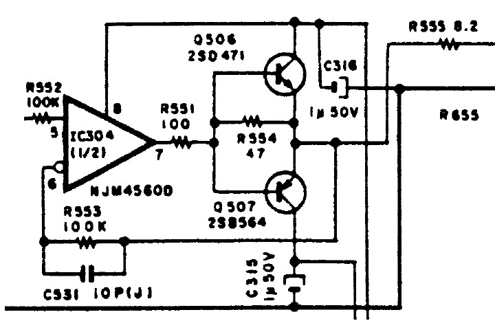 At the last lets look at the headphone amplifier. It is not so important in the design at all because a lot of us use headphones for monitoring. The most precise headphones requires external amplifier and the build in cannot supply enough power and gain. Nakamichi made a unity buffer between the headphones and the line-out of the deck. The buffer use class B high efficiency output buffer. The output impedance is about 8 ohm and it is suitable for low impedance headphones (16-32 ohm). The output is not suitable for the 600 ohm headphones like Beyerdynamic T1. The output complementary transistors is used as current buffer and they start to conduct when the output current from the op-amp is higher than 12-14mA. The buffer is based on high impedance source (R552, R553) which is about 100k. It acts as a insulation between the headphone amplifier and the line out of the deck. Because of its significant source resistance (100k) it requires a op-amp with low current noise. The suitable devices are NJM5532 or the OPA2227. The OPA2228 is not stable in unity gain applications. That is why we replaced the original op-amp with OPA2227.
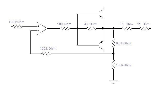 Now the question is how to modify the output impedance of the headphone amplifier to be 100 ohm, which is required by the IEC recommendation, also it is required by the high impedance headphones like Beyerdynamic T1. The answer is very easy by adding additional 91 ohm resistor in series by the output 8.9 ohm resistor. Now we have to increase the gain of the amplifier because the follower cannot supply enough voltage to drive the high impedance headphones. We cut the R553 from the output transistors and connected it to a resistor divider (6.8k by 1.5k). That simply force the follower to increase its gain by the factor of the divider. The gain is good enough to drive the T1 headphones and also to be safe and not to reach the saturation output level which is limited by the 12 volt power supply. The output voltage at Dolby level is about 1.2V rms and the modern metal tapes can supply +5dB so the nominal output level for modern tapes is about 2.13V rms. We have to set the values of the divider (as shown on the previous schematic) that way to prevent reaching the 12V supply limit. The values of 6.8k and 1.5k are good enough to do that.
Switching to ~240V mode
Another important issue is about the power supply voltage. The EU models use ~220V or ~240V power transformer. Most of the machines are set to use ~220V. Since the last power standard defines ~230V as reference on the mains power line then the use of ~220V setting increase the flux in the power transformer. It also increase the hum interference into the playback head caused by the increased power transformer flux. That is why we switched the supply to ~240V setting. The secondary DC voltage after the rectifier now is about +/-17.5V in cassette playback mode, which is enough to drive in safety limit the +/-12V voltage regulator circuit. Before switching to ~240V the secondary rectified voltage was +/-19.6V. The difference between the 19.6V and the regulated 12V voltage is transferred to heat loss and depend by the consumption. Lets assume the typical consumption of ~1A – that means about 15W power loss by heat in the ~220V mode instead of 11W on ~240V power mode setting. For stable work of the regulator the requirements are for at least 3V difference between the input and the output of the regulator. On the ~240V setting the voltage difference is about 5.5V and it is enough to supply the good work of the regulator circuit. On the other hand the reduced power transformer flux is noticeable improvement for the silence moments between the songs.
The phase compensation module
 The phase compensation is another problem for the machine. The problem is caused by the equalization circuits into the recording and playback chain. Most of the machines did not use phase compensation since the pro studio reel-to-reel recorders use phase correction (compensation) into the recording chain. There are several examples for compensation into the playback chain. The Technics RS-B100 was the first cassette model that use phase compensated playback. The RS-B905, RS-B965 and the Tandberg TCD-3014A also use phase compensation into the playback. That means the record still is not compensated and if it is played on non-compensated machine then there will be no effect of the compensation circuit. That is why we decide to make a extension phase compensation module for the Dragon which will correct the phase problems into the recording chain. Then the records made using the recording compensation can be played on non-compensated machine with the proper phase correction.
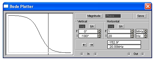
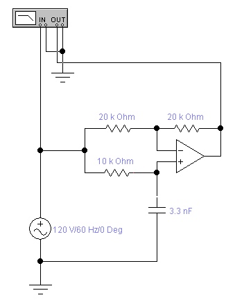
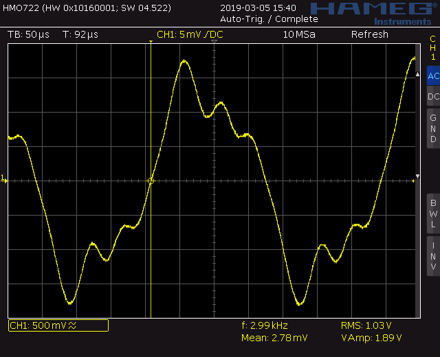
 The compensation circuit use one all pass filter made with additional op-amp, which is connected at the output of the recording Dolby chip (pin 9). As can be seen the circuit affects only to the phase response – note that the frequency response is still flat on the full frequency range. The phase rotation starts at low frequency and is about -153 degree for the 20kHz components. The screen shot of the scope demonstrate the form of the 3kHz square wave at the line out in the monitor mode of the machine (no recording and reproducing by the tape). Note that the true square wave is impossible due high frequency harmonics absence. The summing of the real square wave signal use infinite harmonics, while the real audio chains can pass the high frequency harmonics up to 30kHz. We will inspect the form of this signal when reproducing after the recording.
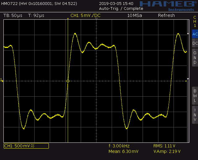
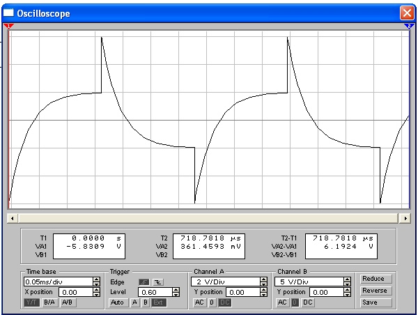 Here how it looks on the scope (simulation) at the reverse compensated square wave signal at the output of the phase compensation circuit. It is complementary to the phase distortions caused by the equalization circuits into the playback and recording chain of the machine. Now let examine the real screen shot of the scope of the 3kHz square wave from the photo above. The first diagram (left side) represents the original recording chain without implementing the phase compensation circuit. The second (on the right side) show the effect when using the phase compensation circuit into the machine. Note that there is no need of switching the compensation parameters for the 70/120uS and also for the normal, chrome and metal tapes due its complementary phase changing in the playback and recording chains.
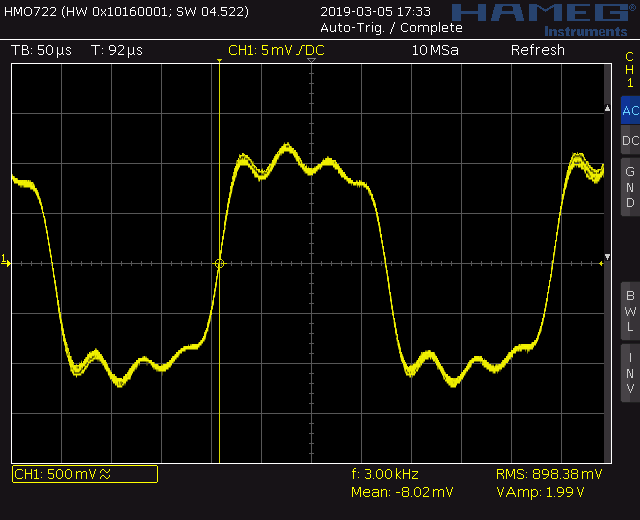
As can be seen the second diagram (on the right) is very close to the original signal (square wave), while the diagram on the left (without phase compensation) use incorrect summing in time of the high frequency harmonics producing the peaks not in the right time.
The 15kHz calibration indicator issue
Nakamichi use peak meter indicator. This is the right way to prevent tape from saturation but the peak mode indicator is also used in the 400Hz and 15kHz calibration mode. The test tones used for calibration are based on sin waveform. The level difference in sin wave between the RMS, peak and VU is as follows: the RMS value is 3dB lower than the peak value and is 0.9dB higher than the average (VU) value. Nakamichi decided to use peak mode for calibration instead of the better average mode to reduce additional switching circuit into the rectifier circuit. What is the problem of the peak detection in the calibration process?
Well, everyone knows that the tape is not ideal media and the tape has dropout when recording. The better tape guarantees lower dropout effects but still there exist dropouts.
Dropout: A dropout is a brief loss or sudden decrease of signal level (volume) most often caused by a defect in the oxide. Dropouts can also be caused by damage to the tape itself, a temporary clogging of the record head during recording, or, likewise, a clogging of the play head during playback. Tape defects can cause frequency-selective dropouts such as a brief loss of high frequency information. Tape speed can be a factor in the effect of tape-defect related dropouts as the condition is less noticeable at higher tape speeds.
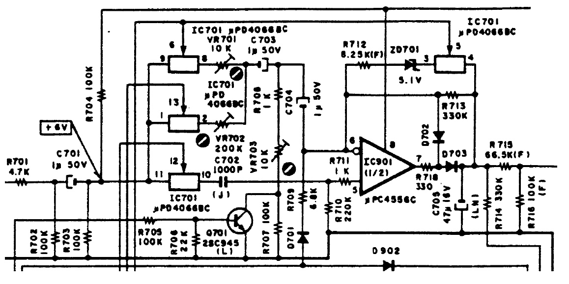 The typical 15kHz dropout is about 2dB. On really good new tapes it can reach 0,5dB. What is the problem with the peak indicator when it is used for the frequency response (15kHz) calibration? It detects the short time peaks in the level and the level calibration is made for these peaks. Most of the time the working level of the tape is lower than these peaks. When the frequency calibration is made with the peak mode indicator then it has high frequency roll off of 1-2dB at 15kHz and 0.5-1dB at 10kHz. It is not so easy to be heard but can be measured with spectrum analyser. The error is very sensitive when using Dolby C system, which is very sensitive to frequency errors. So the right way to set the 15kHz working level is with the average value of the signal, which removes the error caused by the short peaks at plus and minus. Now the question is how to make a switching circuit, which have to be activated only in the calibration process for the 15kHz tone? We will not modify the 400Hz calibration mode because the amplitude of the dropouts for the 400Hz is lower than the 0.2dB and is not so critical for the Dolby level. First lets inspect how the original circuit works. The normal peak mode rectifier is non-linear and is activated by the IC701 (pin 3&4) plus (pin 9&8) switches. The zener diode ZD701 corrects the log scale starting at 0dB up to +10dB. The peak detection is stored by the C705. When the test generator for 400Hz is activated the mention above switches are disabled. That guarantee liner scale for the calibration modes. For the 400Hz the switch (pin 1&2) is activated while for the 15kHz the switch (pin 11&10) is activated. For the 15kHz mode the transistor Q701 is also activated and that set the IC901 in non-inverting amplifier, which gain is set by the value of VR703 plus the value of the serial 1k resistor. For the other modes the IC901 works as inverting amplifier with gain that depends by the resistance of the inverting input (VR701 or VR702). On both modes the only one filter capacitor of the active rectifier is the C705 and there is no way to make it average rectifier by easy changing its value.
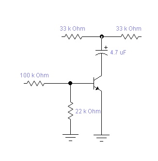 That is why we decide to replace the R715 with two serial resistors of 33k + 33k. At the middle point we placed additional electrolytic capacitor, which is activated to ground by another additional switching transistor. The additional switching transistor is activated by the same controlling signal of the Q701. That ensures activation of the average filter only for the 15kHz testing mode. The left pin of the base 100k resistor goes to the left pin of the R705. That is the controlling signal for the activation of the 15kHz test mode. The left pin of the left 33k resistor goes to the left pin of the R715 while the right pin of the second right 33k resistor goes to the right pin of the R715. The original R715 resistor was completely removed. Note that this mod is made for both channels. So there is another one switching transistor for the other channel plus the filter circuit (33k + 33k + 4.7uF).
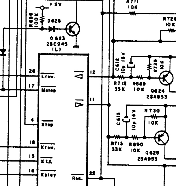
The description will continue with some urgent mods into the mechanism. The first one is for increase the take up torque for a second to prevent problems with take up on very heavy tapes. The second one is for pulling up the tape when changing the tape direction. To explain the mention modifications lets first look at the motor control mechanism and explain how it works.
The tape drive – control modifications
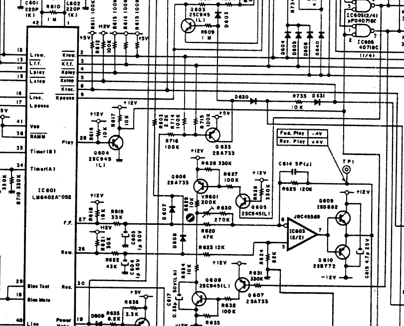
The take up torque is done using one DC motor, which drives the take up hub between rubber idler. Because the machine support reverse mode, then it have to change the directions of the motor. The direction is changed by reversing the voltage of the motor. One of the terminals of the motor is directly connected to the ground. The other is connected to the output of the driver circuit – the emitters of Q609 and Q610. The control processor (IC601) controls the driver that way it sets the different voltages at the output of the driver by the amplifier logic using the different gain of IC603. The pins 27 and 26 of the control processor are open collector based and also used PWM technique to control the different voltage for FF and REV also for the other different modes in Fast CUE and Slow CUE. When the pins 26 and 27 are set to zero it deactivate the CUE or FF/REW mode. It is the stop mode state of the logic. Disabling the conducting to the ground of pin 26 or 27 activates the FF or REW (the direction depends on the pin). For the CUE mode (the slow FF/REW speed) these pins activates 25% PWM mode. For activating the PB mode the mechanism have to reduce the take up tension. It is done by switching on Q606 or Q608 (depends on the direction) and the take up tension is based on the value of the of VR601. The playback activation is done via Q604. It is open collector circuit and when the transistor start to conduct by setting a zero to its base terminal then the motor starts in playback mode.
The increased take up torque on PB start: it is good to increase the torque just for a second at the playback start. This helps to pull the tape on the take up hub and prevents the tape drive for problems. We placed a bipolar capacitor with capacitance of 1uF/50V in parallel to the serially connected VR601 and R630. Now let look how the playback directions are controlled.
The direction is controlled by the second processor (IC602) by the pins 11 and 12. When we change the direction then these pins change it logic to opposite state. These pins control the switching of the Q606 and Q608 and that way controls the polarity of the driver in the playback mode. As mention above, the output voltage is controlled by the VR601. We made a simple circuit extension using two capacitors, four diodes and one transistor to force the PB mode for several second immediately after the direction change of Q602. Why?
Pulling up the tape mod: when the deck change it direction the tape is not pulled because the PB head goes to stop mode. When a new tape is insert then the winding motor is activated for a second to pull the tape. But the problem is that when we change the direction it is not guarantee that the tape will be previously pulled between the dial capstans and this can produce tape drive problems. That is why we decide to add additional circuit to the control logic which activates the take up motor for a second in the similar way like inserting the cassette. The input of the new circuit is controlled directly by the pins 11 and 12 of IC601 and the circuit controls the playback activation transistor Q604.
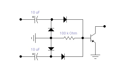
As can be seen the tape pulling mode is quite simple. The positive terminals of the capacitors are connected to the pins 11 and 12 of IC602. The capacitance of the capacitors determine how much time the take up motor will be activated when changing the directions. The collector, which is marked with the black point is connected to the collector of Q604. That way when the circuit detects changing of the direction a current flow through the capacitors and opens the transistor, which grounds the control starting signal. The control starting signal is with inverse logic, so the zero activates the take up motor.
Conclusion
The machine is fully compatible with the last IEC Prague 1981. The measurement of the playback frequency response was done using the Teac MTT-256 test tape. The machine confirm better than the factory specification for the W&F (about 0,015% JIS WTD). The measurement of the W&F of different brands and models cassette and R2R tape decks confirm that the Dragon have the lowest ever W&F compared to the other cassette decks and even better than the most of the R2R at 7,5 ips. The recording is nearly 1:1 with no noticeable difference than the source content. The Dolby level was set to the standard using the Teac MTT-150 test tape. For the reference voltage was used the 387.5mV at the Dolby test point. The meter was set to the true Dolby level at the zero (cal) segment. The most Nakamichi decks are set at 0dB for 200nW/m DIN instead of ANSI method. The MTT-150 test tape refers as 218nWb/m compared to the DIN. The last IEC recommendation for the reference level of modern tapes is about 250nWb/m. As the conclusion we made a short Operating User Guide.
Recommended recording procedure:
Very important! Before start recording please set the mode switches for tape type, Dolby type, MPX filter and 120/70uS switch. It is common practice of forgetting to set the EX/SX/ZX switches on the front panel. These switches set the right bias level and recording equalization circuits and if they not follow the correct tape type then the calibration cannot be done. The meaning of EX/SX/ZX is as follows:
EX – Type I (Normal position tapes)
SX – Type II (High position tapes)
ZX – Type IV (Metal position tapes)
120/70uS switch: You have to switch manually this switch into the recording process. Primary it is type dependent and if you intend to record Type I tapes then you have to chose 120uS and for Type II & IV it has to be on 70uS setting. There are some cases that this switch can be used independently of the tape type. The example is when you use chrome tapes (Type II) and you not want to saturate the tape with high frequency components on high recording levels then you can set this switch on 120uS. It will decrease the S/N ratio but will prevent tape from saturation.
Every time when you use different than the standard EQ settings it is recommend marking them on the J-card of the cassette.
Maximum recording levels:
The ‘0dB’ segment on the display corresponds to the Dolby level, which is 200nWb/m (ANSI).
(I) The first segment above the 0dB correspond to +1dB and it is the recommended operating level for most Type I tapes. In some very short moments the Type I tapes can get up to the second segment above zero (+3dB mark) on the display.
(II) The chrome tapes like TDK SA can be recorded up to +3dB on the display and for some good chrome tapes like TDK SA-X (or better) it can goes maximum to +5dB for short period of time.
(IV) Metal tapes can be recorded up to +6dB on the display and for some short time it can goes up to +7dB segment.
Calibration procedure
Very important: Every time when intend to change the Dolby setting between Off/B/C or when you change the 120/70uS switch you have to start new calibration procedure.
If you continue to record previously played cassette it is recommend opening and closing the cassette door. It will reset the azimuth motor to the reference position. When you start calibration please use the following steps:
1. Activate the recording by pressing the REC+PLAY button. Set the monitor switch to tape. Check for the EX/SX/ZX and 120/70uS. Then press the 400Hz level button. Wait for a second for activation of the 400Hz oscillator. It will not activate the auto azimuth correction. That is why it is recommending to pres 15kHz button to activate the high frequency tone, which is also used by the auto azimuth system. You will see that the auto azimuth indicator will start to blink and you will hear the auto azimuth motor, which will fix the position of the playback head for right azimuth. When the auto azimuth indicator (located on the cassette door) stops blinking then you can continue to calibrate the BIAS setting by the knobs for the left and right channels.
2. When you set the bias level, please set the knobs that way you have stable light on 0dB segment (no blinking) and for some short period of time the first segment above the 0dB (CAL) can start blinking (or weak lighting).
3. When you finish with the BIAS setting then press the 400Hz button and adjust the level knobs that way the 0dB(CAL) segment start lighting. When you finish with the level please go back to BIAS fine readjustment by pressing the 15kHz button and readjust it as described in the (2).
4. Repeat the LEVEL (point 3) /BIAS (point 2) steps several time until you reach the stable LEVEL metering on 0dB and for the BIAS some short blinking of the first segment above the 0dB segment.
5. Now you are ready to press the RESET button and to start with the regular recording.
Mechanism noise
In the working process of the mechanism it is a normal situation to hear the noise comes from the assist and azimuth motors. Here we explain the source of these noises:
1. Power on/off: When you power on the machine you will hear the azimuth motor that zeros the azimuth position of the head lifter. When you switch off the machine you can hear the same motor that tries to zero the current azimuth.
2. When you open and close the cassette door you will notice the same azimuth motor noise. It reset the azimuth head lifter in the insertion of new cassette.
3. When you change the direction in playback mode then the same motor will be activated before starting the playback into the opposite direction. The reason is that it resets the position of the azimuth lifter for the new direction.
4. When the auto azimuth system works then the same azimuth motor is activated until it fix the correct azimuth position.
5. When you insert a cassette the winding motor is activated. If the tape is at the beginning then you will notice it for a second. This is done primary to remove the white tape from the heads and to pull-up the tape between the dual capstans. Note that then you insert a cassette at the middle or at the end of its played time, then the winding force is enough only to pull-up the tape between the capstans.
6. When you change the directions the winding motor is activated for a second to pull-up the tape between the dual capstans.
Warning! Clicking noise on playback
7. The auto azimuth system has no end sensors for the head lifter. The system tries to adjust the azimuth error on the played cassette. If the cassette is recorded with significant azimuth error that is out of the head lifter limits then you will hear a clicking noise of the gear of the azimuth motor. This is weak point in the design of the auto azimuth system but you can notice this clicking sound only on very bad previously recorded tapes. In normal case you should never reach the azimuth final limits.
Future work…
The most important issue were fixed. I’m not commenting the CMOS switch, which I’m planning to replace with good normal signal relays. Still there are 3 important things to do (2 of them are cosmetically and the other one is important issue to be fix). All of them are hard to be implemented and requires significant redesign of the current circuits.
1 Implementing real-time counter instead of simple digital counter: It require a new technique for sensing the hub movement. The lamb into the photo sensors will be removed with IR diodes and the sensing for take up and supply hub will be done by adding another pair of photo transistors (another one for every hub). That will allow to sense the tape direction automatically and it is required for the firmware design of the new real-time counter. The front panel will be changed. The led counter will be extended up to 5 digits (minus for the forward direction).
2 The true peak hold led meter plus RMS reading (combined). Similar to the 1000ZXL and to the 680ZX the display can read both the fast peaks and the loudness of the sound by sensing its RMS value. It requires the design of the firmware for new display controller plus new circuit for rms rectifier and peak sample and hold.
3 The final limit of the auto azimuth system sensing: as mention above there is a clicking noise that comes from the auto azimuth motor when playing a cassette with wrong azimuth outside the final limits of the auto azimuth system. Two sensing sensors will be implemented and if the azimuth head lifter reach the final limits then the azimuth motor will be switched off. It will be switched on if the azimuth correction is at the opposite direction. This will prevent the continuous clicking noise of the azimuth motor.
… and for the final experiment a custom made mu-metal shield will be implemented to the power transformer. It will remove the hum noise.