Part 1 – Introduction
It is a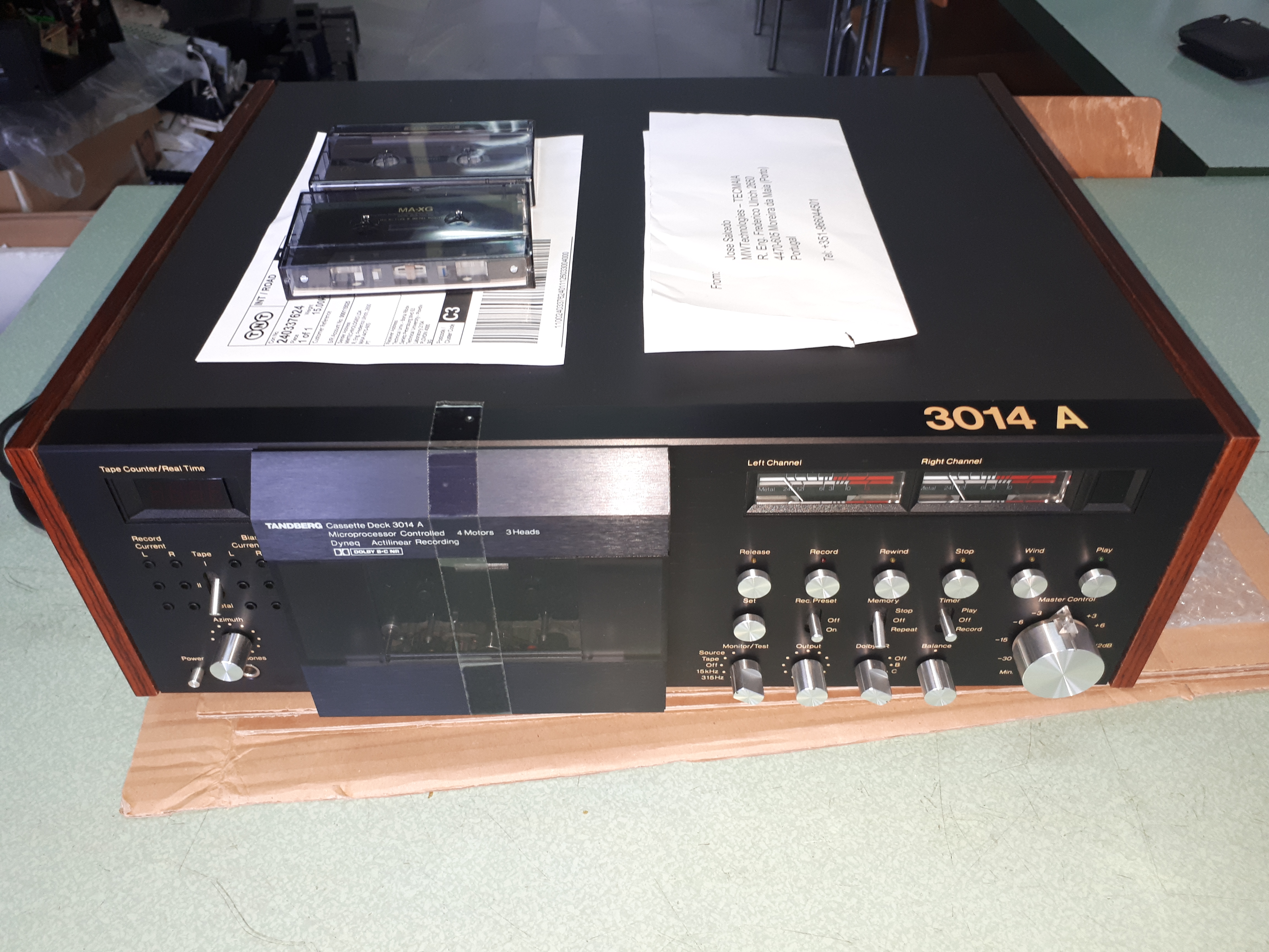 post commenting repair & upgrade process of one interesting cassette deck. I will make a detailed review of this model due to its unique circuit design (reduced use of negative feedback stages). The idea was to repair some problems, calibration, replacing the old parts that grow old and change their parameters. The original playback frequency response of the machine is previously measured with IEC Prague 1981 Teac test tape (MTT256) and it shows full comparison with the current standard that is why the playback frequency response will not be modify.
The machine comes from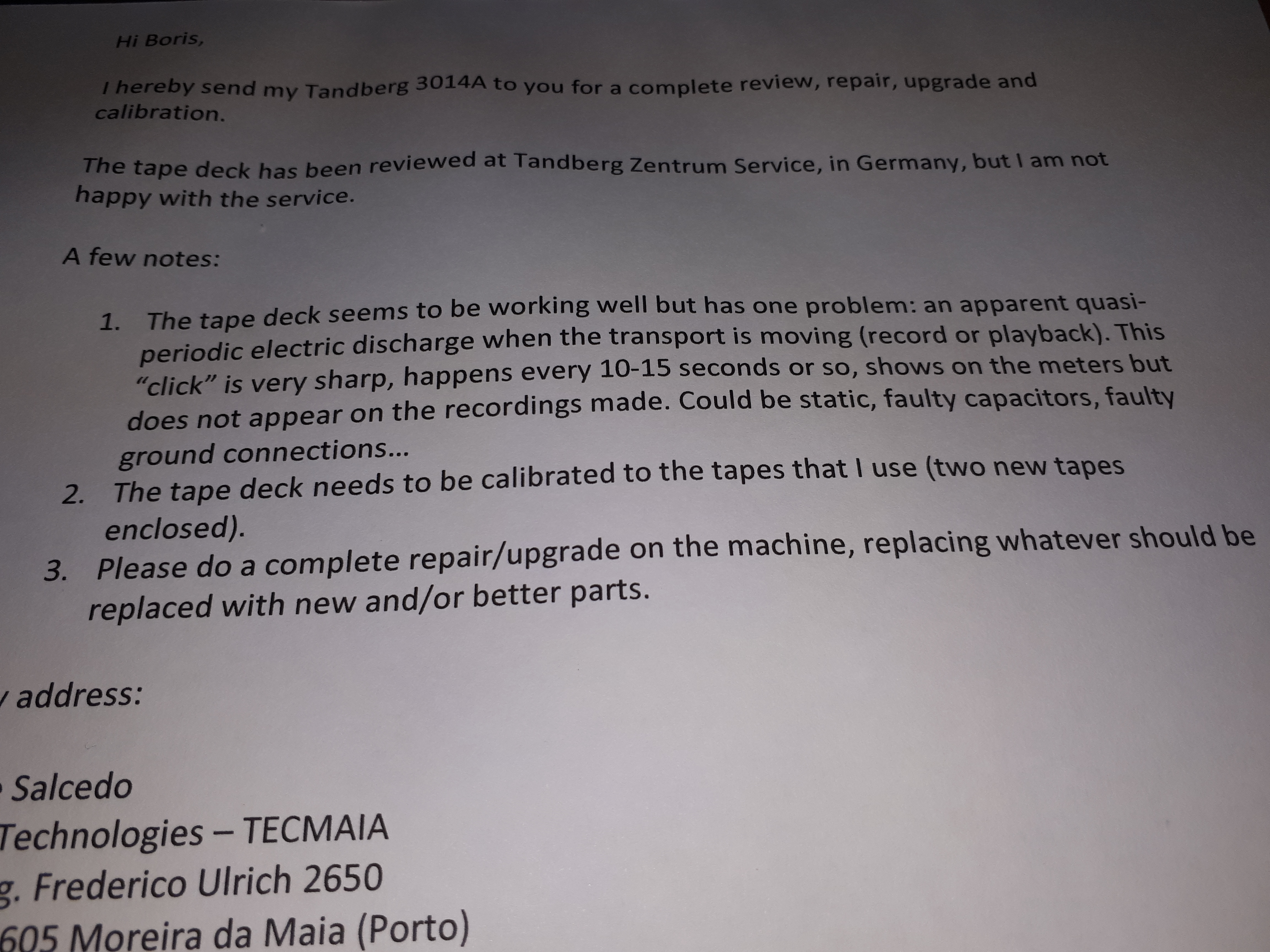 Portugal in very good condition without any shipping problems. The mention problem was about periodic electric discharge on playback. It was previously reviewed in Tandberg Zentrum Service in Germany. At first look the other functions were in normal working condition. Compared the sounding signature with one rebuild Nakamichi 680ZX at first look the sounding was no so interesting. In the past few years I made rebuild process of several 3014A and that is why I decide to publish with detailed explanation why it is required.
First of all, the electrolytic capacitors are 35 years old. Original components are good quality Elna capacitors. The manufacturer guarantee 1000 up to 2000 hours of work at the rated temperature (at 85°C). Aluminum electrolytic capacitor is the shortest life parts in power supplies. This component is the most important parts in terms of reliabilty. Expected lifetime of power supplies can be estimated by calculating the estimation of expected lifetime of aluminum electrolytic capacitor. Expected lifetime of aluminum electrolytic capacitor is determined by amount of excess electorlyte, speed of electrolyte evaporating through sealed rubber and temperature that determines the evaporating speed. The relationship between ambient temperature and capacitor life has been confirmed to follow ARRHENIUS’ equation:
Expected lifetime of Electrolytic Capacitor:
L = Lo x 2^(T1-T2) / 10 ,where:
Lo : Lifetime Under Maximum Rated Operating Temperature (Hr)
T1 : Allowable Maximum Temperature (°C)
T2 : Capacitor Temperature on operation (°C)
 In other words, life of aluminum electrolytic capacitor is temperature dependant and it is doubled when ambient temperature is 10°C lower, based on Arrhenius’s Law. Life expectancy is determined by a coefficient depending on temperature, based on Lo. Detailed explanation can be found in the technical note of Rubycon Corporatin: CapLife
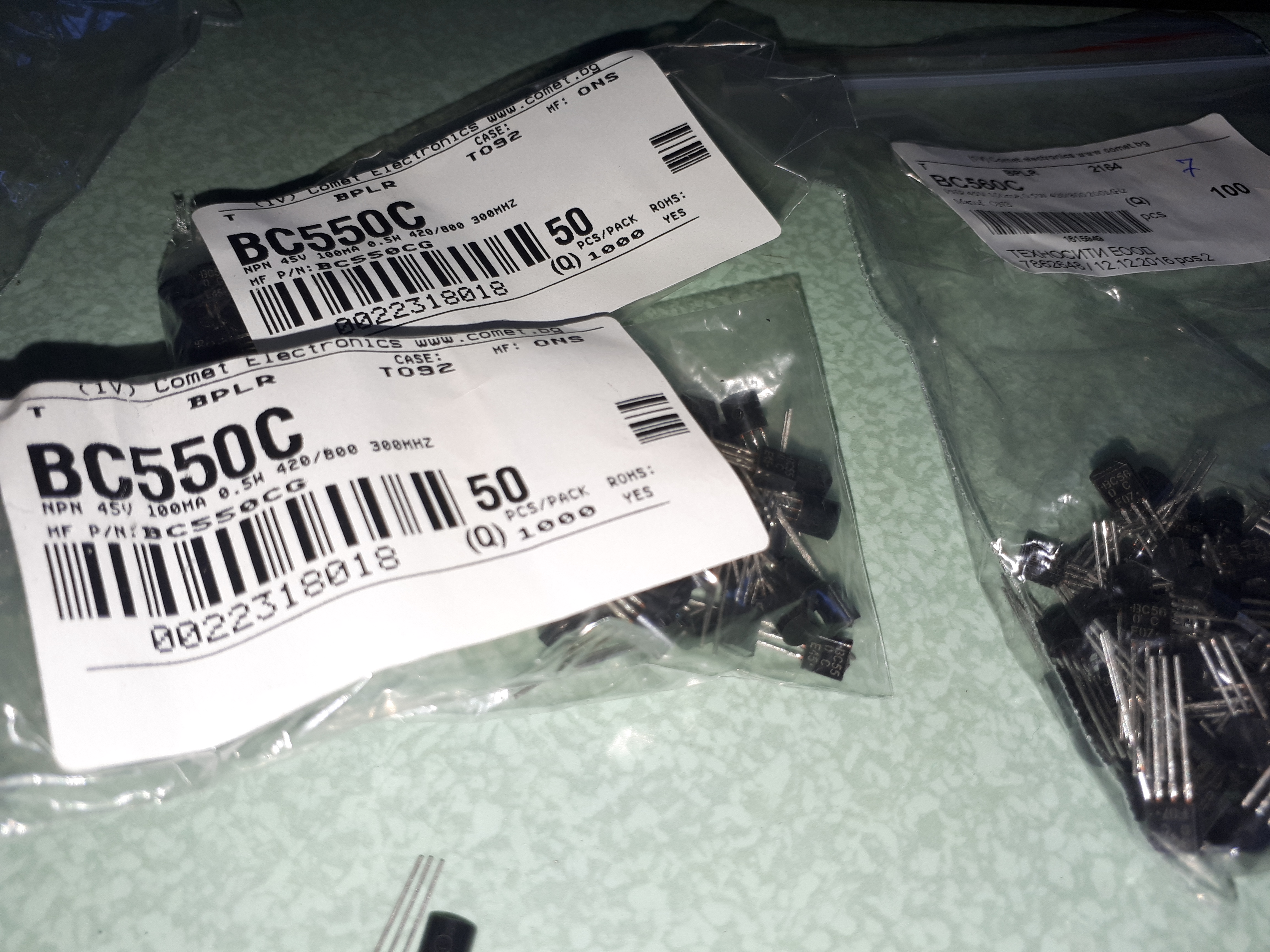
Lets make a simple calculation. If the capacitor is used in temperature of 25 degree its life will extend with a ratio of 64. It is about 128’000 hours for a rated cap of 2000Hr at 85°C. Is is about 15 years. That is why I always recommend to replace all of the Electrolytic Capacitors in the equipment older than 20 years. So I ordered the proper caps from Mouser – the power caps I use are Panasonic FC type and the signal caps are based on Elna Silmic II. Noticed that several biggest manufacturers of audio equipment (like MBL high-end audio and Accuphase Laboratory Inc) use the same type of capacitors in their designs and products. I also decided to replace some critical caps with bipolar depend on the circuit. In this article will be explained the oversize and the critical part replacement for every component in the machine.
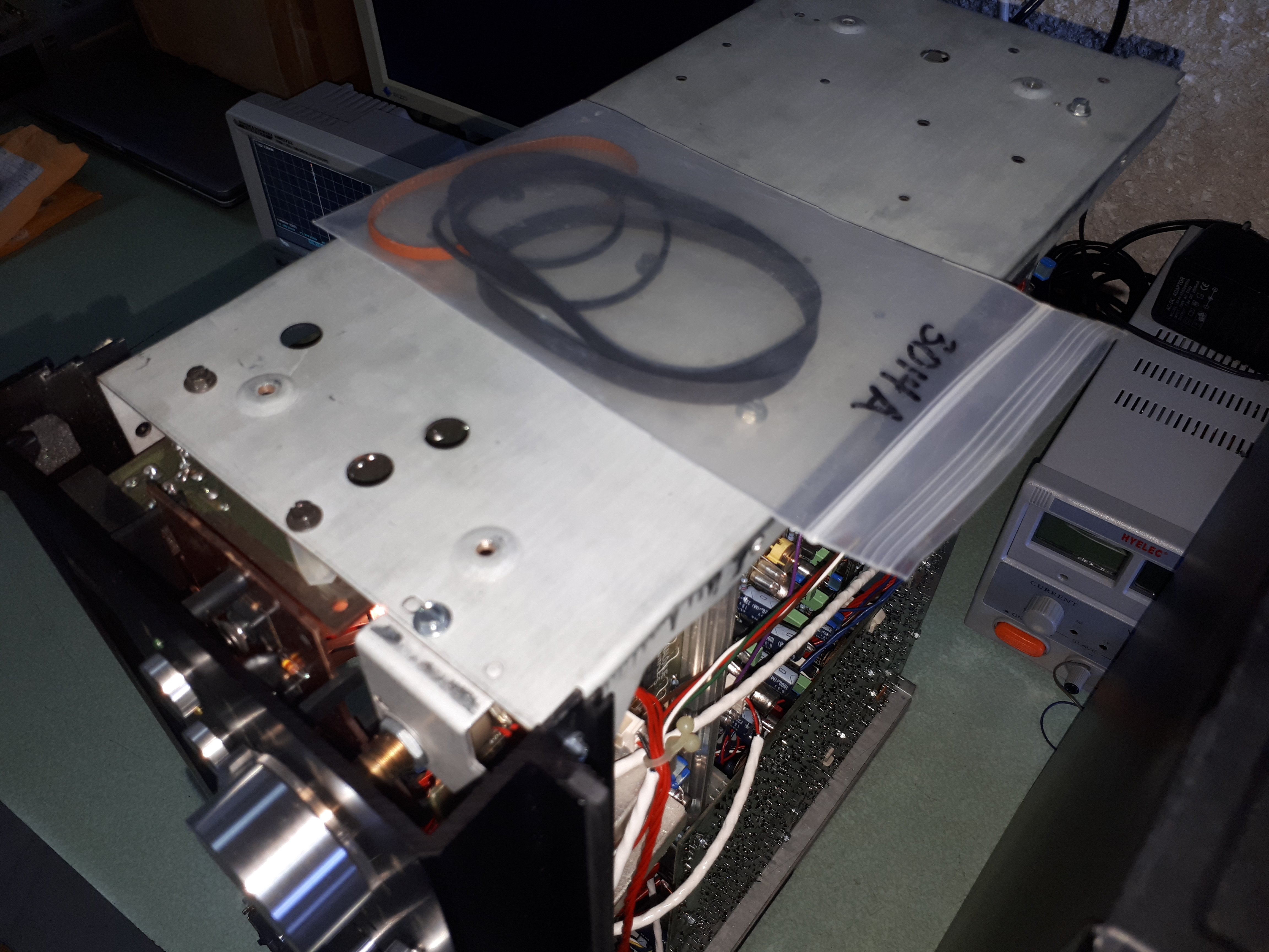
Looking at the mechanism of the TCD-3014 I noticed that the flat belts are in working condition but the square belts for the take up and supply hubs are weak. I decided to order new kit from Marrs Communications (previously I tested their belts for different TCD-3014 machines). The cost of this kit from US takes about 78 USD as in my conversation with Krista:
The Kit is in stock $38.75, plus Priority International Mail. $39.95 for UP to 10 Kits.
Please follow this link to the correct page on our website to Purchase
http://www.marrscommunications.com/tandberg-cassette-r-r-and-azimuth-belts
Thanks Again,
Krista
 Making a combined shipping I was able to get it for 60 USD including the shipping. The main reason to order full belt kit is that flat belts on the others 3014 machines that I have done were in bad condition. The replacement is not so easy and it is good to be done when the mechanism is rebuild. In a few days all the parts of the mechanism will be disjoint, take to pieces, cleaned, fresh lubricated and reassembled.
Meanwhile it is time to diagnose the electrical discharge problem and some improvement into the circuit. Tandberg decide to use transistor of a type BC547/BC557 . In the year of production the lower noise BC550C/BC560C were cost ineffective. I decide to replace all BC547/8/9 and BC557/8/9 marked with B or C rank with BC560C and BC550C. Note that there exist some places that the replace is not suitable and I will note about it.
There 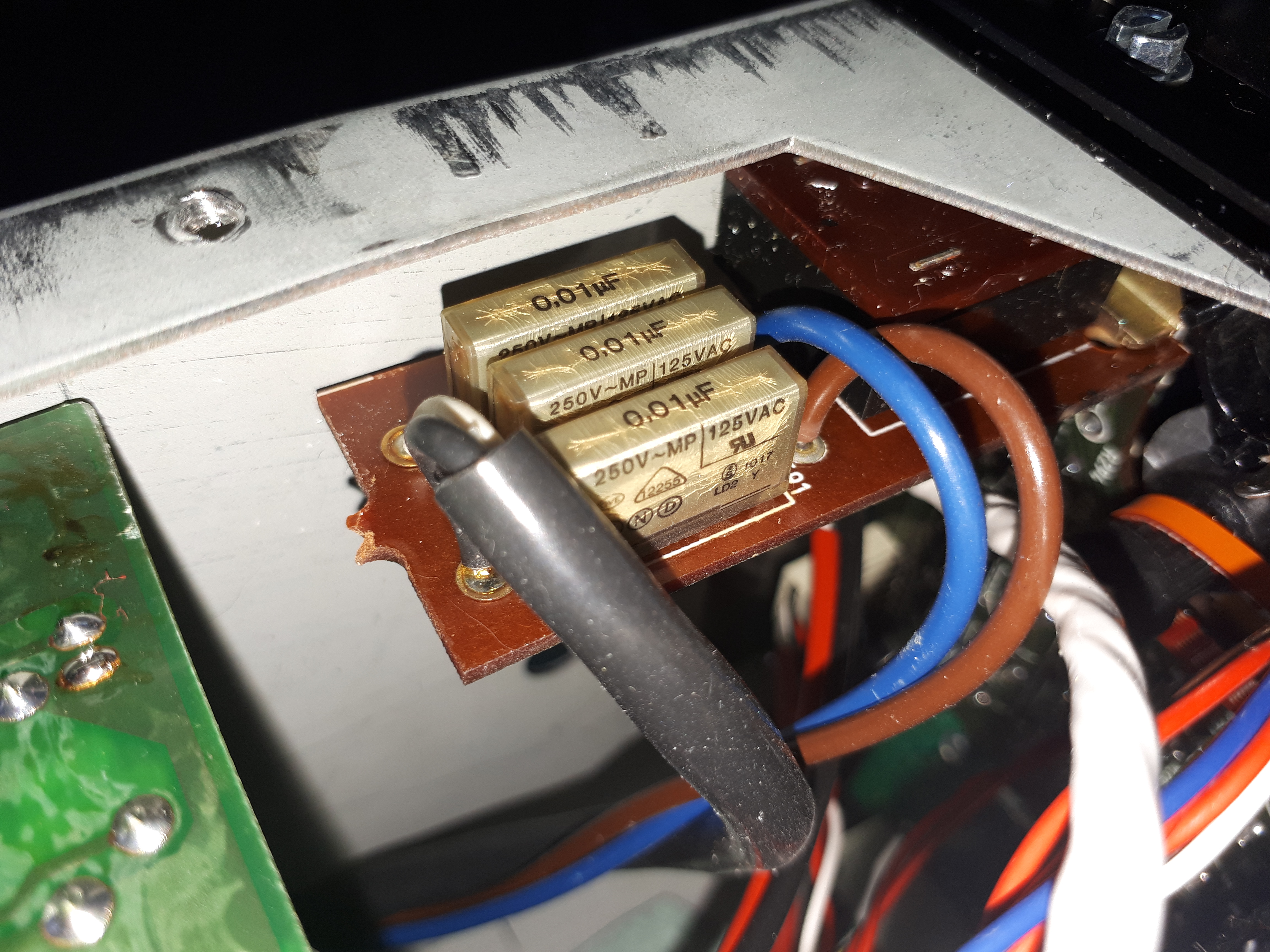 are also some RIFA X1/Y1 caps in the power supply that are damaged and is required to be replaced. The RIFA caps are also know as “ticking time bomb”.
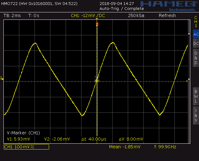
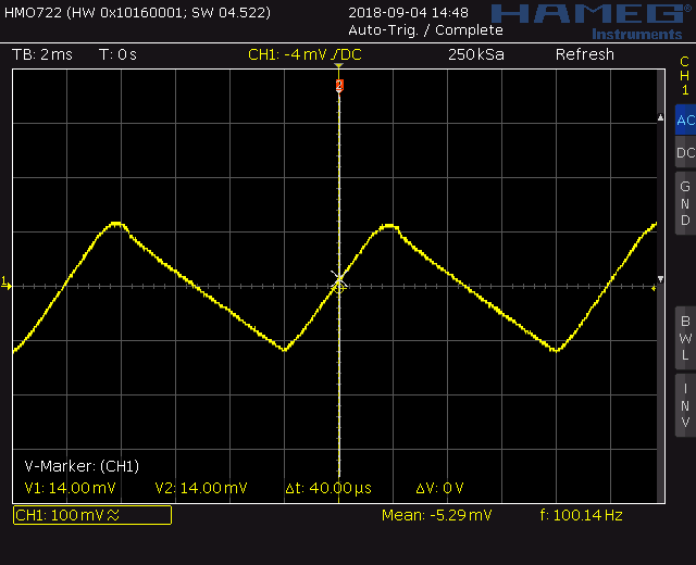
The power supply electrolytic capacitors are one of the most important part in the audio. It is better to oversize their capacity. One reason of the fact it is not done in the design of the machine is that the higher capacity caps are too expensive for regular production. The measured ripple from the power supply using the original capacitors was about 500mV (0.5V). It can be seen also on the snapshot of the scope. When replacing the power caps over their capacity the ripple was reduced up to 200mV. It is significant improvement because some modules are powered from the non regulated supply (for example the variable output amplifier and the headphone amplifier. The second part of this post will describe the schematics and when it is good to oversize a capacitor.
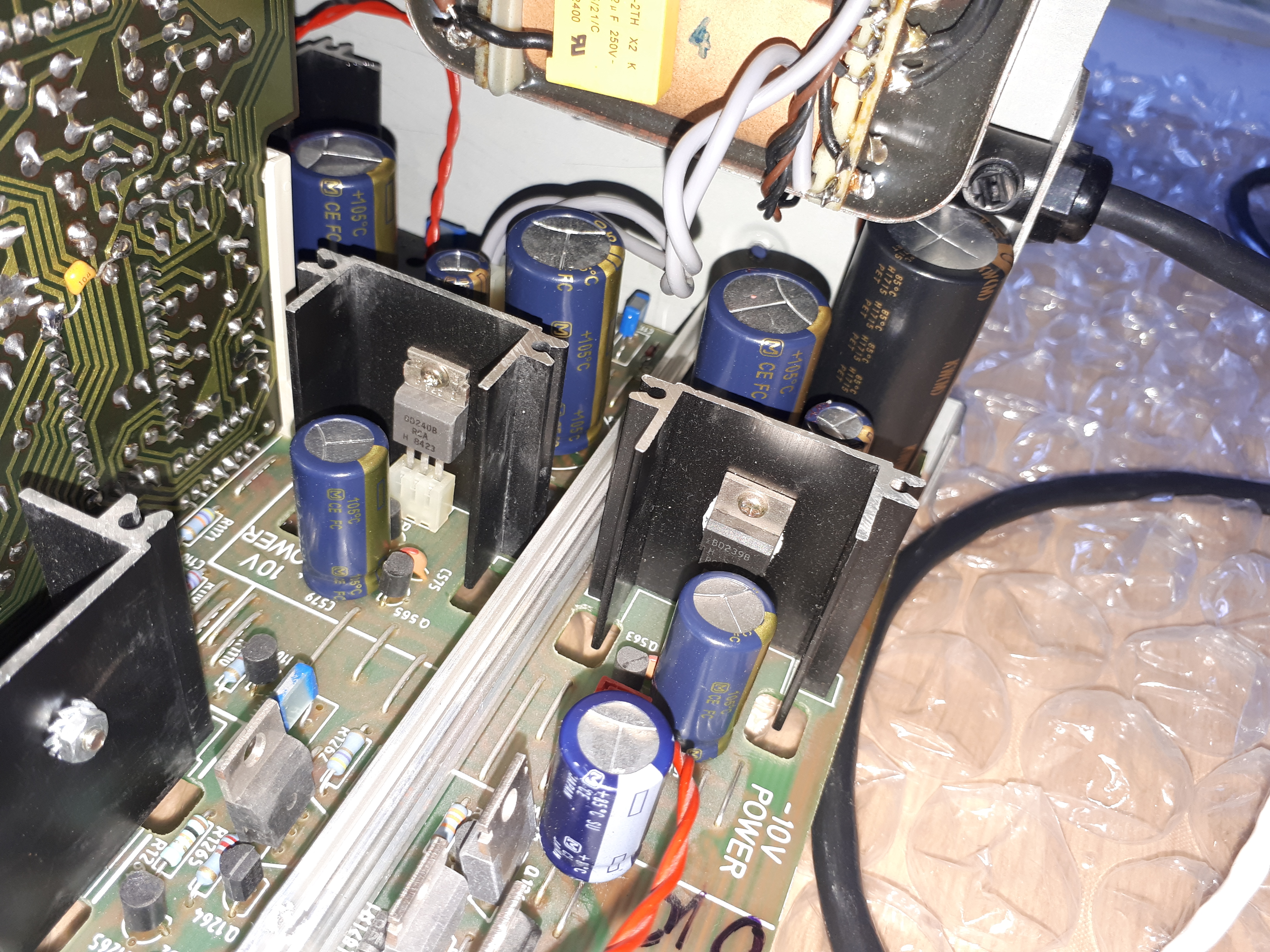
 There is another yet grounding problem in the machine. The construction consist of two main PCB connected together with detachable connectors. These connectors are used for the power supply exchange and when the contacts are dust with oxide the noise from the power supply take a interference. It is good to solder with hard connections between the two main boards as shown on the photo. The reference ground point of the PCB is where the rectifier filter caps for the positive and the negative are connected together. It is good to set this point for the chassis ground.
Part 2 – Schematics review
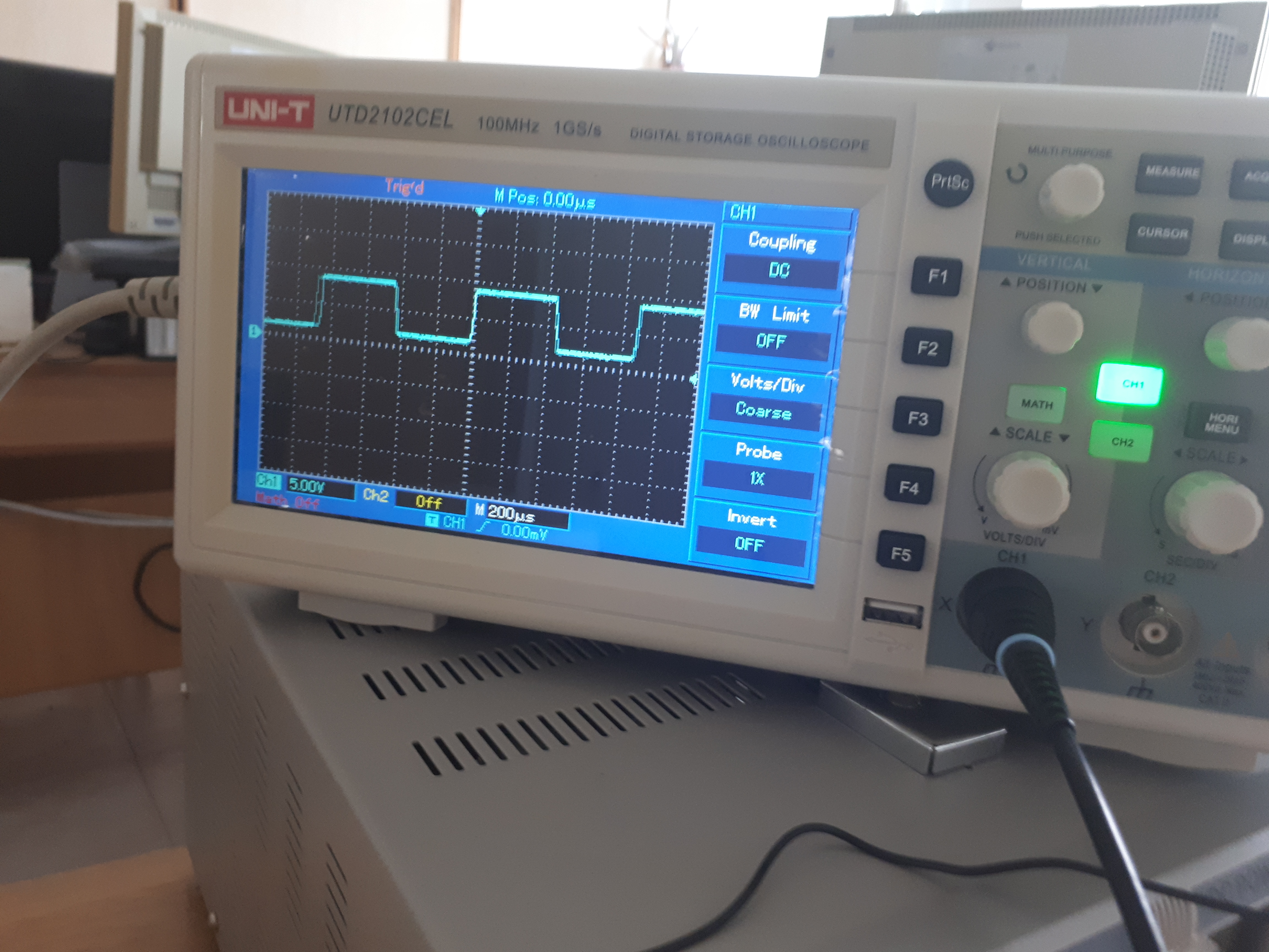
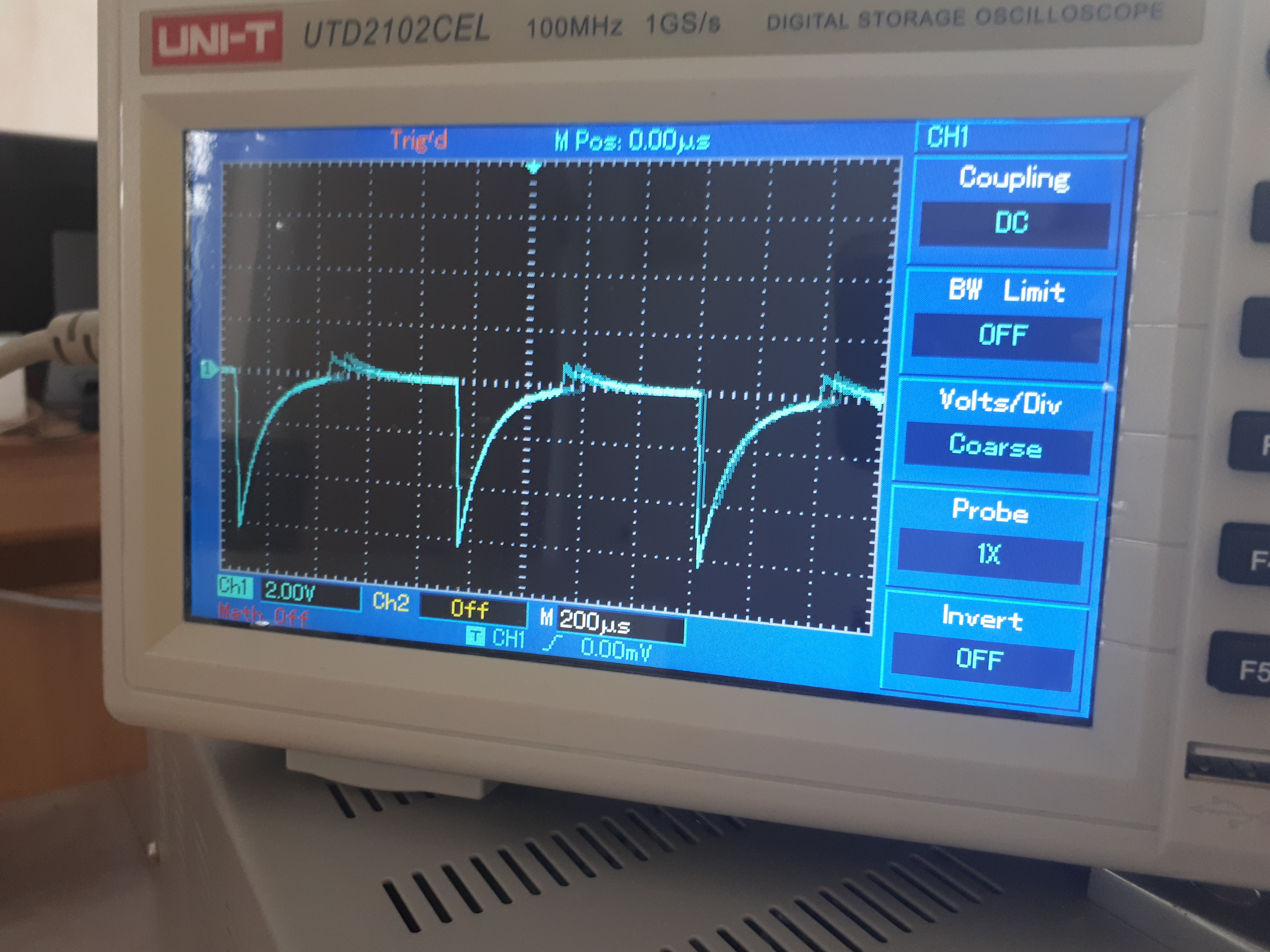
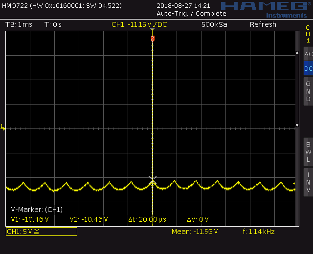
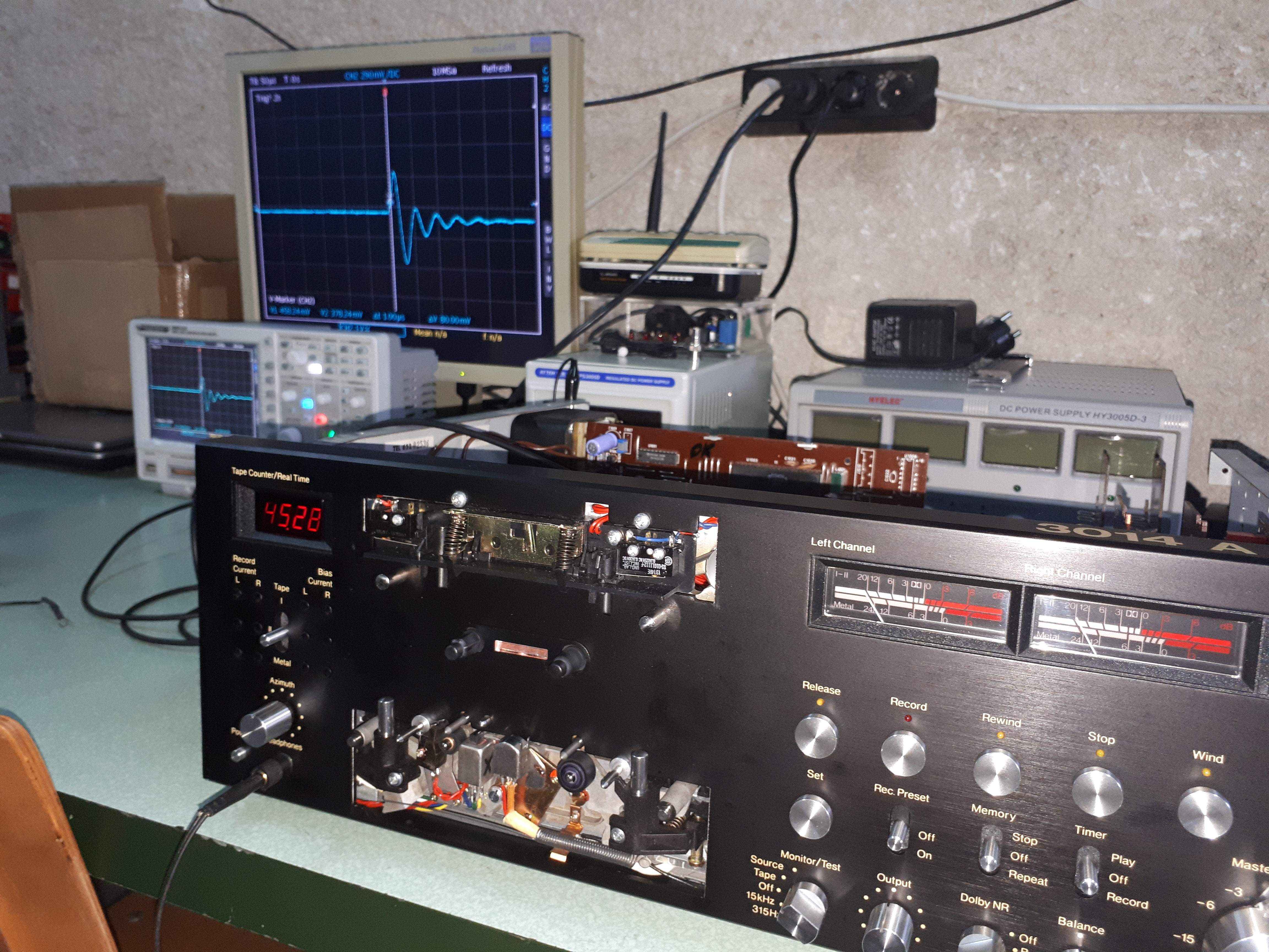 Before any further work on the machine it is good to repair the existing problem with the electrical discharge on the playback. It can be seen how it looks like on the scope. The investigation show that it comes from the playback amplifier and exists on both channels. I suspect some filter caps on the power supply. As can be seen it looks like DC charging the output and in some time this small DC charge clears in a oscillation process. One can decide that it can be due leakage transistors in some high impedance circuit. That is why I decide to replace all of the planned transistors in the playback chain. After the replacement the problem still remains but the sounding of the PB amp stage and the unity gain buffer amp improves its slew rate. The used low noise transistors with its higher gain shows noticeable improvement on the sound signature. The electrical discharge problem do not comes from the head. It exist even on shorted playback head input and disconnected head. The investigation show some spark pulse on the mechanism control motor. In first look that suspect problems in the control processor. The signals that control the position of the mechanism comes from 4-bit discrete external D/A converter. A small spark pulse exists on the output of the D/A and set the servo control circuit to make a large integration pulse on the mechanism control motor, maybe to a digital glitch caused by the control program. When the mechanism motor activates it generate high current consumption from the power supply and more noise and interference. In normal playback mode the motor is in static mode and do not generate noise and power supply peaks. That is why the output of the D/A converter was filtered with small 330nF poly capacitor. The final conclusion confirm that the spark interference comes from bad capstan motor. When it is disconnect then the ‘spark’ problem disappear. There are several confirmations for wear out capstan motors (the same motor is used in AKAI GX77).
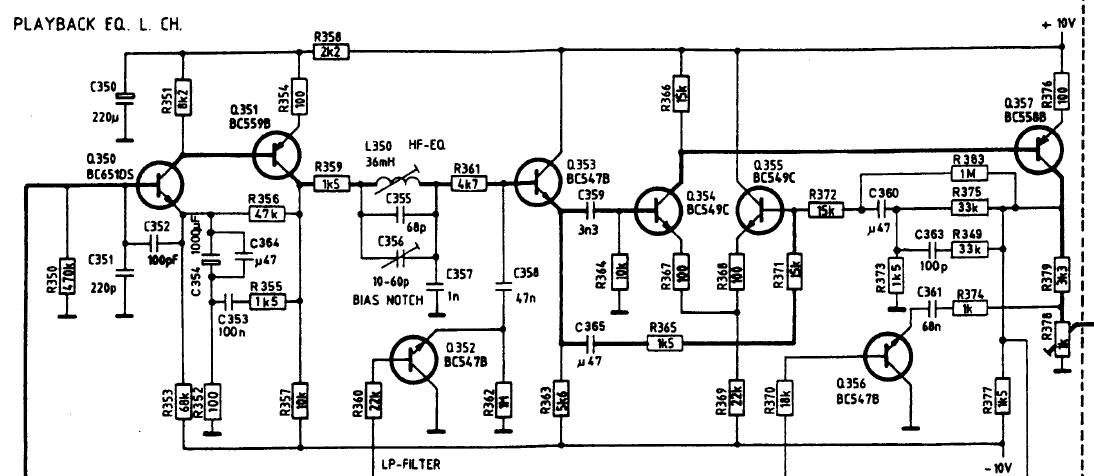
Lets look at the playback EQ amplifier. One have to be noted that it is playback phase compensated. That kind of approach is used in few cassette decks. The playback phase compensation also is used in Technics RS-B100/905/965 decks, while the recording phase compensation is used in Revox B215. TCD3014A use playback phase compensation and it helps the previously recorded tape without phase compensation in the recording to be played properly on TCD-3014A. Most of the prerecorded tapes are not phase compensated in the recording process. The phase compensation (all-pass filter) is done in amplifier with the following transistors: Q354, Q355, Q357. C359 and R364 determines the starting point of the phase rotation. The switching time constant between 120uS aud 70uS is done by Q361 at the output of the playback amplifier. The head is connected directly to the base of the first amplification transistor and there is no any coupling capacitor between. It is recommend to oversize the C350 in range of 820-1000uF and the type Panasonic FC. For the C354 it is good to use 1000uF Elna Silmic II. Both are well polarized so it is not required to be BP caps. The Q352 changes the HF playback roll-off of the input amplifier in stop, fast forward and rewind mode (also on program search modes). It is required because of the cue function of the deck. When it is in stop mode and the stop button is hold on by pressing the fast forward or rewind the searching function is activated. The number of pressing the fast forward or rewind button simultaneously with the stop set the number of the searched track on the tape. All the transistors except Q350 were replaced with BC560C and BC550C (depends of their type).
Mod tested by Boris Ribov: Everyone who is interested to test the replacement of BJT transistor in the input stage with the JFET 2SK170GR can read the following modification section. This is a simple mod and the primary goal is to remove the large electrolyte capacitor in the sensitive parts of the amplifier (C354). The second goal is to use the best approach for the input stage – one JFET with its lower potential input current and voltage noise that will improve the S/N ratio. The same way will be removed the DC current flow to the playback head and this avoid any head magnetization in time. First replace the Q350 with the 2SK170GR. The emitter have to be replaced with source terminal, the base with the gate and the collector with the drain. Short the C354 (short circuit). Remove the R353. Replace the R351 from 8.2k to 44oohm (it will be required to set it in test mode between 300ohm and 560ohm). Reducing the resistance from 8.2k to 440ohm also reduce the thermal noise generated by R351. Place a electrolyte capacitor in parallel to R354 with the capacitance of 470uF/6.3V. The plus terminal should be connected to the upper side of the circuit and the minus to the emitter of the Q351. That is all – the following mods will reduce the interference and distortions comes from C354 and the second will decrease the self thermal noise of the R354.
 The signal of the playback amplifier goes to the Dolby playback (expander) circuit, which is placed in separate board. The board will be review later in this publication. The reference Dolby level of the test points is referred as 700mV using the Tandberg test tape (1kHz, 0dB = 250nWb/m). The specification of the chip confirms the 580mV on the test points if used Teac Dolby test tape MTT-150. There exists supposition that the reference level specified in the service manual is wrong listed but we made test bench that confirms the listed value in the manual. Detailed explanation can be seen in another article that can be found here. The signal that comes from the output of the Dolby decoder goes to unity gain buffer. After the buffer it goes to the fixed out RCA connector and to the volume control resistor of the headphone amplifier which is the variable output amplifier.
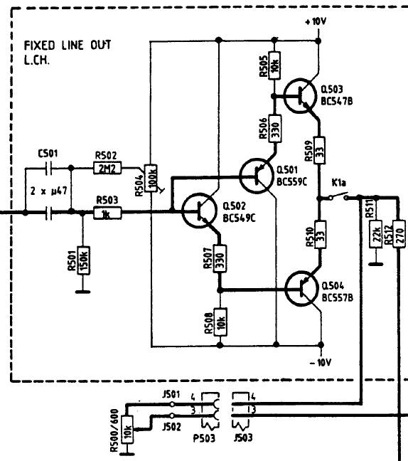
Lets look at the buffer circuit. As can be seen it is very close to the diamond buffer design. What about the ‘sounding’ of the capacitors. The’ sounding effect’ is caused primary by the distortion of the signal passed into the capacitor. There are several confirmation that if the current passed through the capacitor is reduced then the harmonic distortion is also reduced. If a capacitor is connected to high impedance circuit and input then the current passed into the capacitor will be reduced. The unity gain circuit is based on 150k input impedance and two parallel 0,47uF good poly caps. It is probably the best solution avoiding use of electrolyte capacitors. The DC offset at the output is set by biasing of the input transistor by R504. The output is directly connected to the RCA line-out plug using just one serial resistor of 270 ohm (R512). That approach avoid use of large electrolyte coupling capacitor at the output to reduce the harmonic distortion. Removing the output coupling capacitor is possible because the zero offset voltage of the output, which can be trimmed by R504. Two major modifications of the circuit are made. First all the transistor pairs were replaced by BC550C/BC560C. Second the output serial resistance, which determine the output impedance of the RCA line out is replaced from 270 to 100 ohm. The lower output impedance is better to drive the high capacitance interconnects. For example the capacitance of the line out cable is in the range of 75pF – 250pF per meter. If it is used long cables of 2 meters then the higher capacitance of the cable tends as low-pass filter and the output impedance determine the HF cut-off frequency.
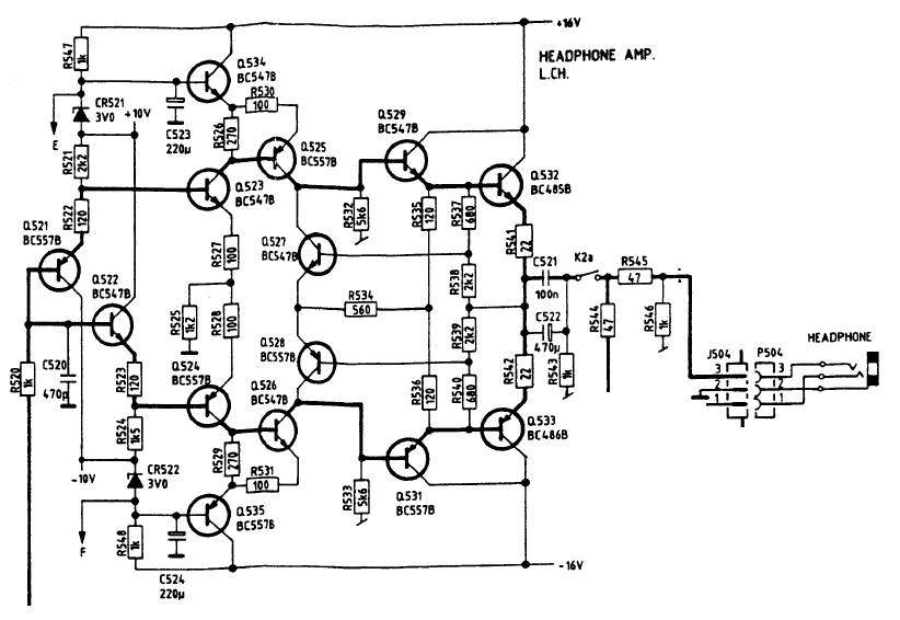 We will continue this review with the variable output buffer and amplifier. The same time it acts as a headphone amplifier. The circuit implements diamond buffer structure in the front and reduced use of negative feedback. The main disadvantage is that is use large coupling electrolyte capacitor at the output. This capacitor is also polar. Thinking that at the time of producing the machine the bipolar capacitors were exotic components. To decrease distortion in the output capacitor it have to be polarized. Looking at the circuit it is fully symmetrical. Measuring the DC voltage across the output capacitor it is about 1,9V. The amplitude of the audio signal at full output level is about 4V and is not good enough but for lower signal levels the polarization voltage is enough to reduce the distortion of the output capacitor. The increased distortions in high output level are not so sensitive to the human ear. The team that designed the 3014 was absolutely right to use this approach. Similar approach is used in the Nakamichi BX-300E and MR1 cassette decks, where there exists several virtual ground and the capacitors DC offset is about 6V. It is interesting where comes from the DC offset in the symmetrical design of the headphone amplifier. If we look close to the circuit will notice one difference in the R521 and R524. A small difference from 2.2k compared to the 1.5k give the DC output offset. It is good approach but the same way increase the signal distortions and maybe not so much compared to the distortion of the non polarized polar output capacitor. The modification we made are based on replacing the R521 with 1.5k instead of 2.2k (precise value trimming is done for zero DC offset at the output). That way the DC voltage at the output will be close to zero. The same time we replaced the C522 with large bipolar capacitor. Looking at the output impedance of the headphone amplifier it is about 47ohm (determined by the value of R545). We will replace this resistor with 100 ohm to ensure 120 ohm output impedance. As several people know that there exist a recommendation for the output impedance for the headphone amplifiers. The 1996 IEC 61938 standard defines 120 ohm output impedance and is followed by several European manufacturers like Revox (in the model B750), Phillips, Beyerdynamic, etc. The recommended output impedance of the T1 headphones manufactured by Beyerdynamic is about 100 ohm. Changing the output impedance will change the damping factor and the frequency response of the driver of the headphones. The summing output impedance (impedance of the amplifier circuit plus the resistance of the R545 will give a value of 120 ohm for the headphone output impedance. Basing on the 100 ohm serial resistor will calculate the minimum value of the coupling capacitor (C522) for the lower frequency roll-off. The capacitance is no lower than 1000uF /6.3V to ensure good low frequency response at the output.
And what about the improvement of this circuit: it is recommended to replace the C523 and C524 with capacitor 1000uF/16V (we placed Paansonic FC). These capacitors are filter of the reference voltage regulator for the Q534 and Q535. There is no 100nF in parallel to these filter caps but if we look at the PCB we will note that there are soldered two 100nF capacitors in parallel to the diodes CR521 and CR522. They are enough to filter high frequency interference because the second terminal is directly connected to the reference power supply. We replaced most of the transistors (except Q532 and Q533) with measured pairs of BC550C/BC560C. Note that you also have not to replace the Q525-Q528 with higher gain transistors. If you do that the circuits will start to oscillate at 60MHz. We measured serious amplitude about 4V and 60MHz at the output with high gain transistors for Q523-Q528. That is a confirmation for the good slew rate and bandwidth of the headphone amplifier. There are only several op-amps that can be used in the amplification mode up to 60MHz.
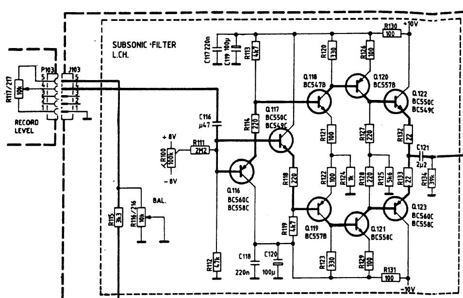 Going to the schematics of subsonic input filter. It is not switchable. It is a impedance buffer (high input and low output impedance). The cut low frequency (7.2Hz at the input and 5.6Hz at the output) is determined by the input impedance (R112) of the buffer and the next stage impedance and the values of C116 and C121. Removing the ultra-low frequency component avoid the noise breathing (modulation) in recording. Changing the Q116/7 with BC560C/550C (originally placed BC549/559) improve the circuit. Also replace the Q122/3 with pair of BC550C/560C. One noticeable problem is with the stability of the circuit. Setting the input volume to minimum or setting it to the maximum and the balance knob to minimum can cause interference (hum) at the output of the buffer. It is caused by small oscillation at very high frequency about 100MHz. It can be avoid using one of the following approach: placing in series to the center pin of the volume control a resistor of 1-2.2k; or you have to place a filter ceramic C0G(NP0) between the terminals emitter-base of the Q116 and Q117. The suitable capacitance is between 33 up to 100pF.
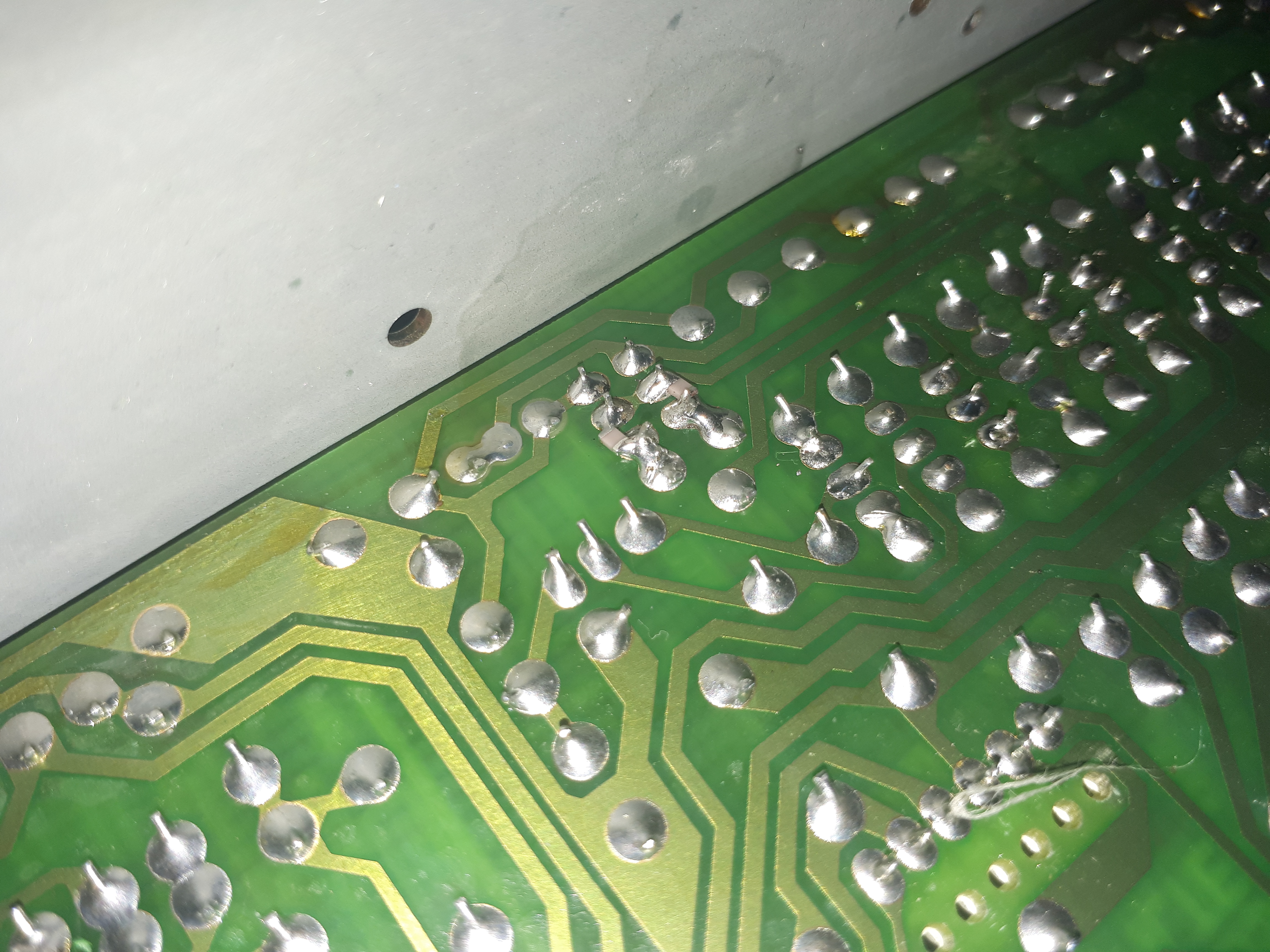 This approach will remove the ‘hum’ noise caused by the ultra high frequency oscillation and increased current into the buffer stages caused by the high frequency oscillation. Also it will remove the input radio frequency interference of WiFi and GSM mobile networks. This interference cause rectifying the radio signals into the base-emitter junction. Placing a small capacitor in parallel to the junction simply remove the amplification and rectify effect of the junction. You can see how the small SMD (0805 footprint) looks like when soldered at the bottom side of the board in parallel to the base-emitter terminals.
The TCD-3014 implements new recording technology called Actilinear II. The traditional Actilinear system works as a separate recording equalizer which is followed by current driven recording amplifier. The high frequency bias into the recording head is traditional and the bias trap is required between the output of the recording amplifier and the recording head. The inductance of the bias trap increase the impedance of the record head circuit and that affects the headroom of the high frequency components. The Actilinear II system works similar to the crossfield technology used in several reel-to-reel decks. The recording head is connected directly to the output of the recording amplifier without bias trap.
 That kind of approach use additional bias head in the opposite side of the recording head (in the R2R decks). There is no easy way to make crossfield into the cassette deck, so the bias signal feed the input of the recording amplifier. That way the recording amplifier gains both the audio signals and the high frequency bias signal. The mixing is done in a passive resistor network. That kind of approach use linear current mixing without any additional IMD distortions in the non-linear components. Tnadberg notice that the recording amplifier acts as voltage to current converter. It has enough headroom to compensate the increased impedance of the head for the bias frequency and to supply the required current to the recording head. It requires fast and wide bandwidth recording amplifier to satisfy good signal amplification of the 85kHz bias component. The reference bias and level points are set by trim-pots separate for the left and the right channels for the 3 common used tape types. The mixed signal then goes to the input of the recording amplifier. At first look it is a traditional differential amplifier. The recording head is connected to the output by a large electrolytic capacitor. This capacitor removes the DC component to the head and that way removes any additional nose into the record cause by any DC offset.
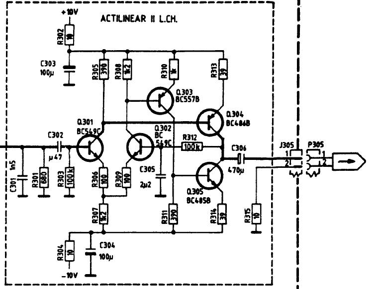 The capacitor C306 needs to be low ESR capacitor due to the high HF current passed into the recording head. The recording amplifier is a zero DC output, so we replace this capacitor with 1000uF bipolar from Nichicon. Also a PP cap with 10nF value was placed in parallel to the C306 and C406 to ensure low impedance for the bias frequency. The bipolar capacitor reduce the distortions of the low frequency audio signal. If we look at the circuit we can notice that it is a non-feedback on AC. The feedback works only for the DC signals to ensure zero volt output. The feedback input is shorted for the AC signals by C305. The stage works on class A with low distortion and the highest fixed possible gain. We replaced the power filter caps (C303 & C304) with low ESR caps and oversize the capacity to 820uF/16V. We also placed additional PP cap in parallel to the C303 and C403 to ensure low power impedance for the bias frequency. We changed the transistors Q301 and Q302 with the lower noise BC550C.
 These transistors acts to the linearity and need to be selected with equal gain. That is why we made a precise selection of different lot of 100pcs. The same is with the front transistors in the recording amplifier.
The recording amplifier is done using inverting amplifier circuit. The first two transistors acts as differential amplifier, one of the input of the amplifier is connected to the ground. The output of the first differential amplifier come to the second stage amplifier (Q153). The load of Q153 is dynamic and it is a current source generator. Both the resistors in the positive and the negative power circuit are low impedance (R159, R161). That ensure very high dynamic range of the recording amplifier.
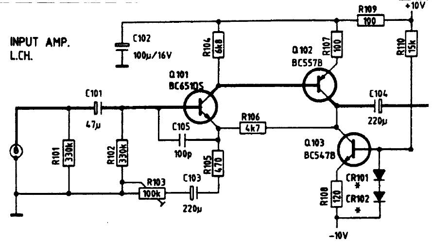
 The required equalization is done in the feedback network. The low frequency boost is done using C153. The high frequency compensation is done using T filter circuit (R152 and R158) and the middle point connected impedance to the ground. The compensation is done for normal tape (Type I) using L151, C156 and R169. The value of the R169 determine the HF boost and the required compensation. The right terminal of R169 is connected virtually to the ground. It is connected to the diode switches CR15 3 -CR156, which are part of the DYNEQ system. In normal work these diodes are forced with high enough current and their dynamic resistance is very low. The required compensation for the chrome tapes (Type II) is done using transistor switch Q155 and the circuit C154 and R164. It is required to change the value of C156 for the flat frequency response on recording for most contemporary tapes. The compensation circuit for the metal tapes (Type IV) is done using the switch Q156 and the elements C155, R167. The output of the recording amplifier use coupling capacitor C153. It is a polar capacitor and it is better to replace with Elna Silmic II. This capacitor is polarized by 0.6V and works good in that kind of circuit. We placed a film WIMA PP capacitor in parallel with capacitance of 10nF.
 Let see how the DYNEQ system works. First we can see that it is level dependent by the type of tapes that we use for recording. The switching transistor for the metal HF EQ compensation is connected with Q159 and are both are switched in the same time for metal tapes. The Q159 determine the level at witch the DynEQ system is activated. For metal tapes this level is higher compared to the normal and chrome tapes. The DynEQ system sense the output signal from the recording amplifier. It pass to a high pass filter to select only the components which cause the tape saturation in the recording. It the power of the HF components is too high then the Q157 is switch on and decrease the current that pass to the diodes CR153 – CR156. That way it increase its dynamic resistance to the ground and disables the boosting circuit L151, C156 and R169. That way it prevents the tape from additional over saturation. It is described in the next diagram:
If we look at the input amplifier will see that is well designed. The output capacitor is polarized with a voltage about 1.5V DC which is enough at the typical signal levels of 700mV at the output of the input amplifier. The output is loaded with current source (Q103) about 6mA quiescent current working in class A. The circuit is not push pull and cause significant second harmonic distortion compared to the push pull ones. The push pull designs removes the second harmonic but cause significant third harmonic. The approach to use that kind of input amplifier is based on the fact that the spectrum of the natural musical instrument tends the linear fading in the spectrum by frequency. That means the second harmonic of most musical instruments has bigger value than the third one. That way the distortions caused by the amplifier have more natural sounding signature than the distortion caused by push pull symmetrical amplifier.
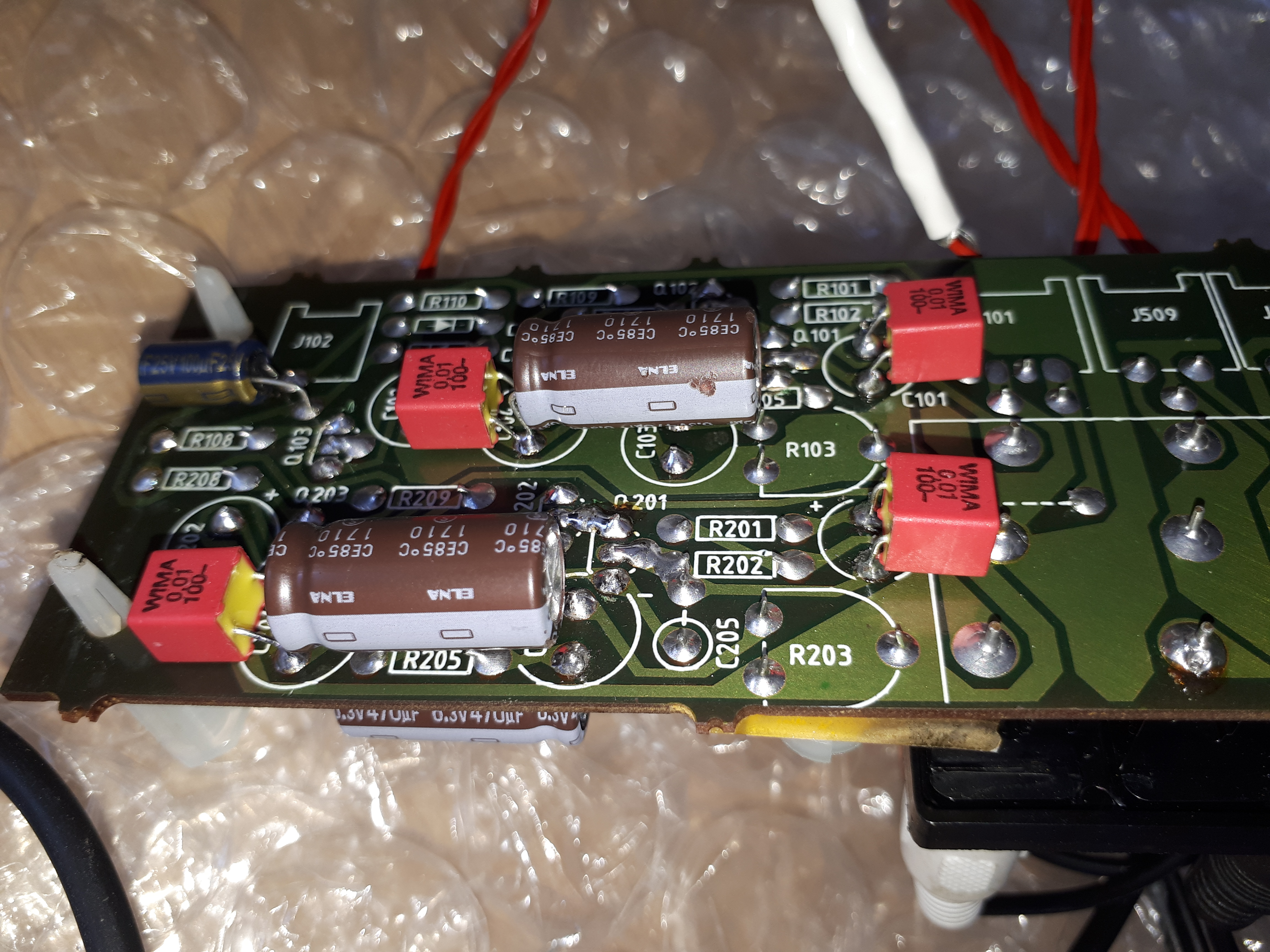
 The input capacitor of the amplifier is also polarized with the bias current of the first transistor. The DC voltage is about 80mV. The suitable replacement for the C101 is 47uF/16V Elna Silmic II. The voltage at the emitter of the front transistor is about -0,6V which also set the DC bias voltage of C103. It is required to place a 10nF Film PP capacitors in parallel to the C101, C103 and C104. C102 is low esr type and did not require a PP cap in parallel. Also change the C103 and C104 with 470uF/6.3V Elna Silmic II will extend the low frequency response which is not so noticeable but corrects the phase linearity of the low frequency range. C102 is oversize with Panasonic FC type 820uF/16V. It is good to place in parallel to the power connector of the board a 100uF/25V between the +10V and -10V terminals. A good approach it to replace the transistors with BC550C and BC560C pairs. Here it is how it looks the input amplifier after the improvements.
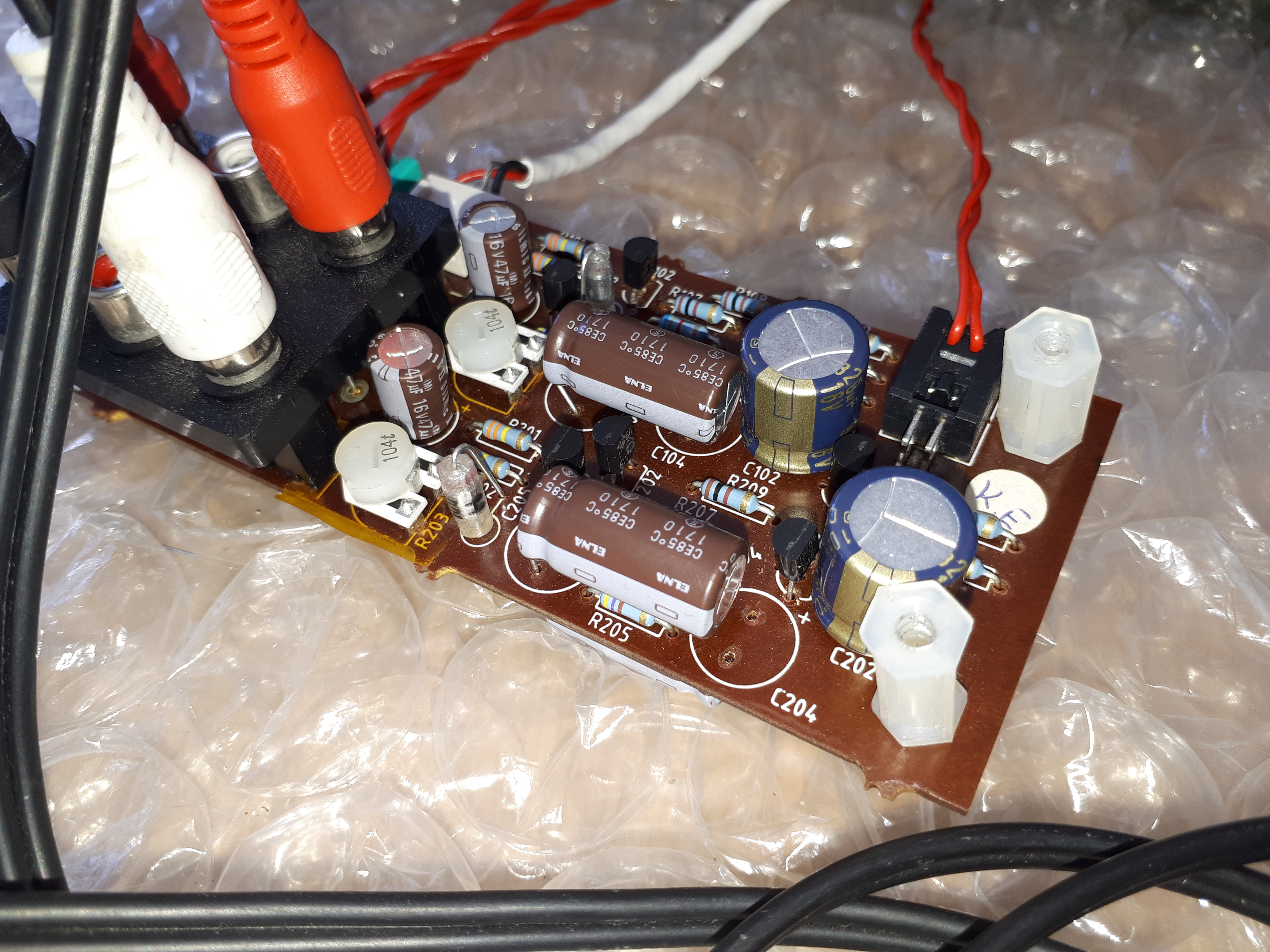
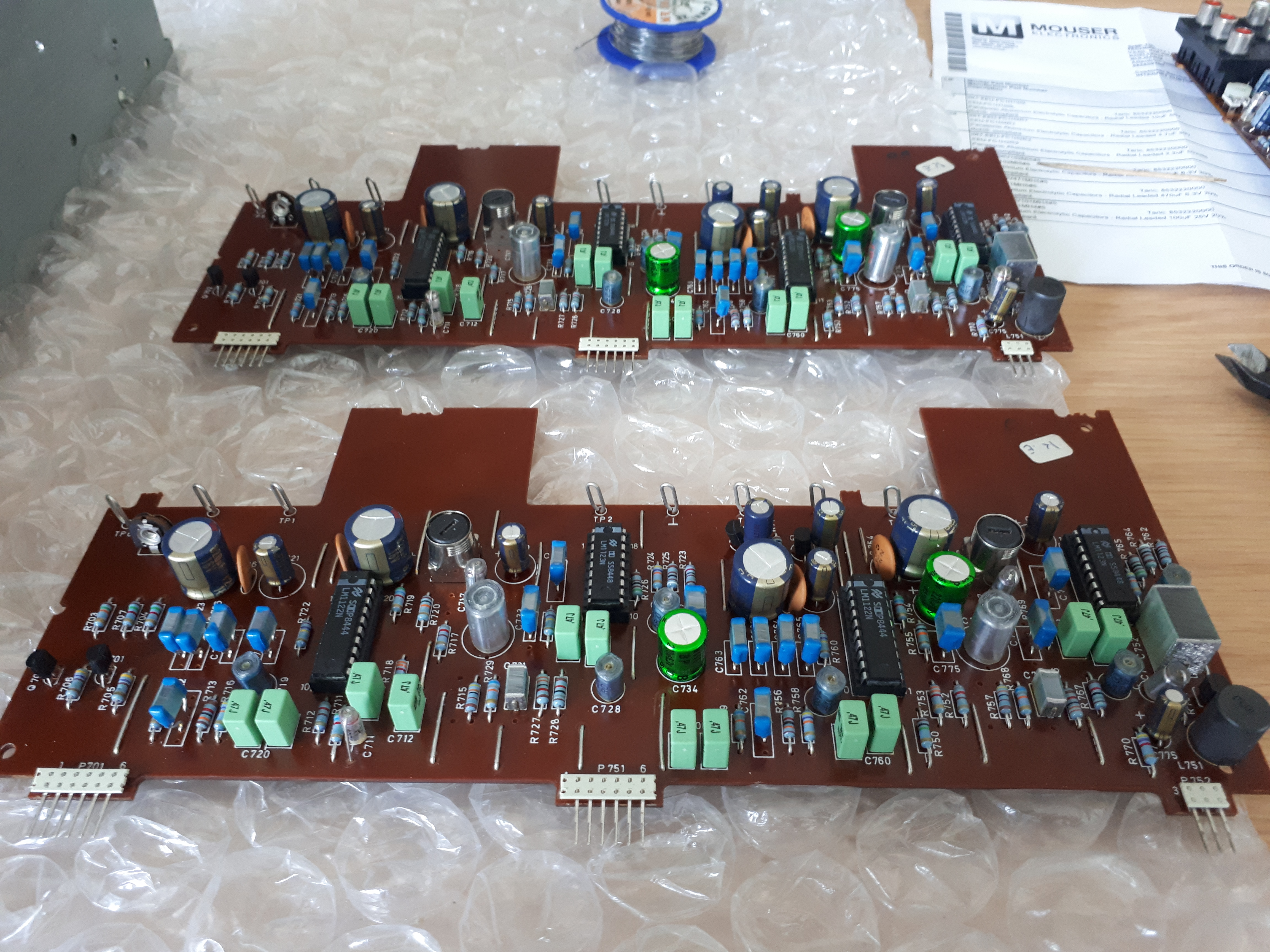 The Dolby modules of the deck are placed on separate boards. The Dolby chips are made by National Semiconductors. The chips tend to be improved version of Dolby B and C compared to traditional chip manufacturers. The module is well designed in separate boards for the left and for the right channel. The circuit of every board is split for the playback (decode) and recording (encode) modes. It is good to oversize the power caps to 820uF/16V. There are only two caps in the signal path that are not polarized and it is good to be replaced by bipolar (the green ones in the next photo). On the power supply regulator it is better to set in parallel two caps of 100uF/25V to the zener diodes.
 The power supply module use traditional feedback regulated design. It is good to oversize the first rectifier filter caps to 5600uF/25V and the rail -V to +V cap with 6800uF/50V. Similar to the Nakamichi approach at the output of the regulators we place large capacitors of 2200uF/16V instead of used 100uF. The local filter caps C871 and 872 are replaced with 1000uF/25V instead of used 100uF. Also the zener bypass caps are changed from 10uF to 100uF/25V. That approach reduce the ripple in the power supply.
Another interesting module in the 3014A is the Peak Program Meter (PPM). The meters use full wave peak detector and in recording mode is connected to the output of the recording equalizer. That way it shows true recording current and prevents the high frequency saturation. The response is about 2mS peak about 1dB. The way they are connected is interesting. In normal mode when the REC ON switch is deactivated they monitor the source and tape output at the line out terminal. If the REC ON switch is activated then the PPM meters monitor the recording equalizer. That is why the tuning of the meters is not so easy. I will describe the special procedure that I use for accurate meters also including the Dolby system complementary. As I said previously the Dolby chips use reference levels at 580mV (400Hz) at the test points. When all the other alignment is done (frequency response, azimuth, speed, zero point at the amplifiers, Dolby playback level) then follows the final procedure for the PPM meter. First of all we need to supply the Dolby complementary for the playback and the recording. Ensure you switch off the Dolby system switch and supply the line input with 400Hz signal. Set the line input level and balance that way you get a 580mV on the output of the Subsonic filter (that is also the input of the recording Dolby module). Then set the trim pot R702 on both Dolby boards to get 580mV on TP2. That ensure the complementary of the recording Dolby module with the playback Dolby module that is previously tuned with the Teac MTT-150 test tape.
The second step is to set the zero point of the PPM meters. As mention early the zero level for the TCD-3014A is 700mV (1kHz). Because the internal level generator is based on 315Hz it is good to use 315Hz at the line in for setting the reference level instead of 400Hz. Supply the line in with the 315Hz and set the input level and balance in that way you get 665mV at the line TP2 point of the recording Dolby board. The Dolby system has to be switched off and the REC ON switch also has to be switched off. It is better to do this without a cassette inserted into the deck (that prevents the PPM meters to be connected to the recording equalizer output). The 665mV is the reference level get from the Teac IEC level test tape. Set the trim pots R562 and R662 that way you got the 0dB reading on the display.
Third step is to insert a blank cassette ready for record. Set the REC ON switch. The Rec led will start to blink. Now the PPM meters are connected to the output of the recording equalizer. Set the trim pots R561 and R661 to get the 0dB reading at the meters and to make the reading equal with the step 2 when switching the REC ON switch on and off. Now you have to set the test generators levels.
Forth step is to insert a blank tape for recording. You need a spectrum analyzer to ensure the flat frequency response on -20dB. It is done using the bias knobs on the front panel for left and right channels. Ensure that the recording azimuth knob is set to the peak position. Then apply a 315Hz at the line input of the cassette deck. Set the level knobs at the front panel that way you read the same level at the line out when you switch between source and tape when making the recording. That will ensure you set the right parameters for the recording equalizer. Not you have to set the test generators. Switch on the 315Hz test generator and set the reading of the PPM meter to 0dB using the trim pot R138. Then switch the test generator to 15kHz mode and set the reading on PPM meters to 0dB with the trim pot R140. Ensure that the 315Hz test mode is also on 0dB. That is all. You set the machine for the flat frequency response and zero IEC level.
Part 3 – Mechanical repair & improvement
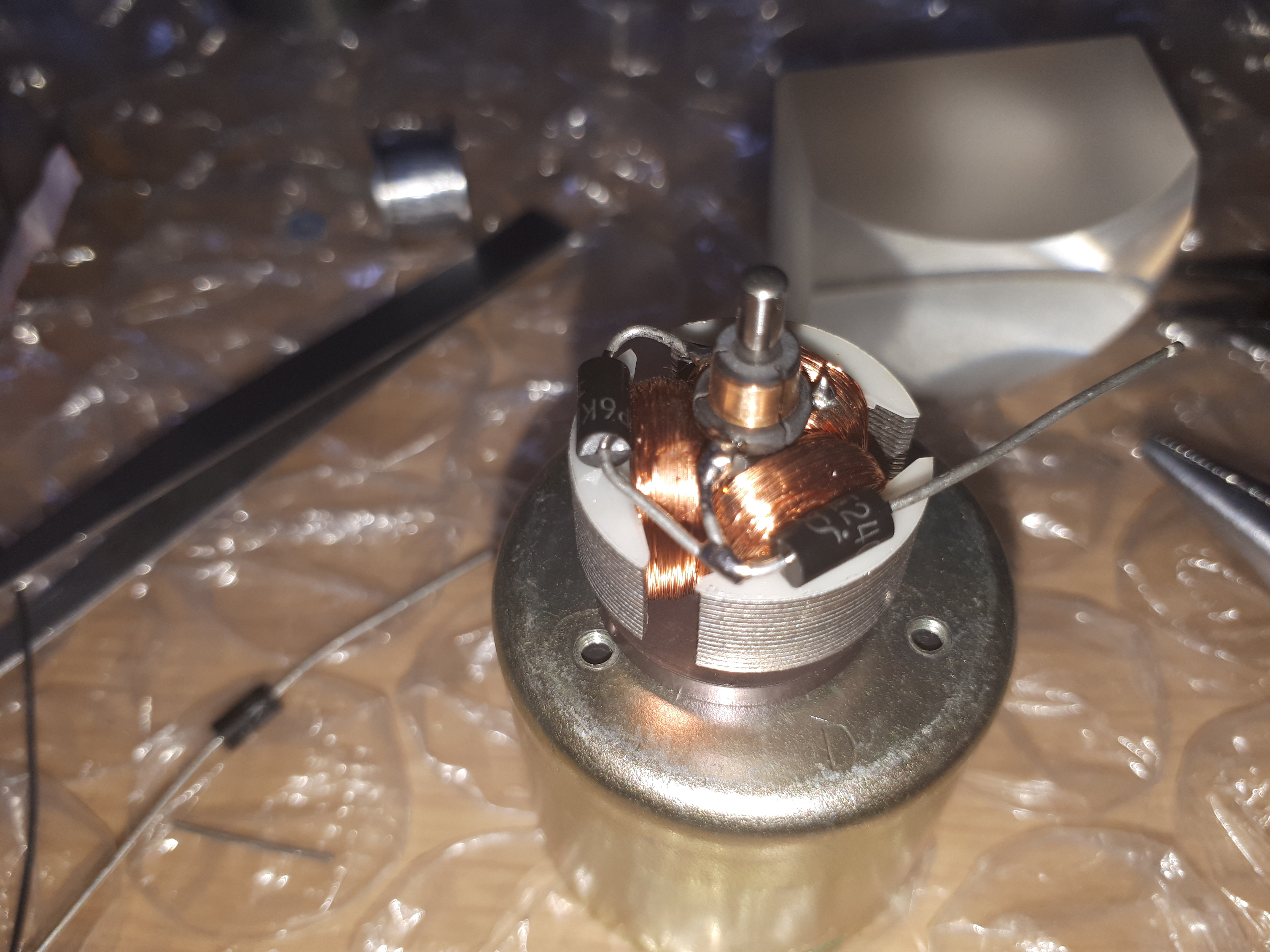
The most interesting part is the capstan motor and the improvement of the motor radiated noise. As it was mention at the top of this review, there was existing ‘spark’ noise problem in the playback which cause bad discharge noise in period of 5-6 seconds. The investigation confirm that it comes from the capstan motor. That is why the motor was disassembled for cleaning and lubricating. The construction use two metal chassis, which are isolated from the metal ground of the deck chassis.
 There are two permalloy shields also between the internal and external metal motor shields. The motor use sintered bush which was lubricated. The full absorption of the oils into the bush take about 24 hours. It is good to be lubricated and to be assembled in the next day. The motor use traditional 3 conductor design in the commutator and external tachometer gear for speed control loop. The commutation in rotation of that kind of motors generate spark or arc in the conducting process. To reduce the EMI noise of the sparks in the rotation a ring varistor is used between the terminals of the commutator. The varistor is designed to start conducting at voltages higher than the 14V. In the commutation the inductive part of the motor coils tend the current to continue when the circuit breaks in the commutator. This switching cause the high voltage and the spark.
 The varistor start conduction and 14V and suppress the spark and arc. The short time high voltage is absorbed into the varistor as a heat. It can damage the ring varistors in long time use. That is why we replaced the used varistors with 24V bidirectional Transient – voltage – suppression (TVS) diodes. The leakage current which is higher for the Varistor particularly close to the knee of the curve. The slope of these characteristics in the clamping zone (vertical part of the curve after VBR), here one can easily see that the Transil™ diode slope is tighter than the Varistor one. And taking into account that the curve slope represents 1/ Rd , so for the same surge current the clamping voltage will be lower for the Transil™ and then its clamping factor will be better.
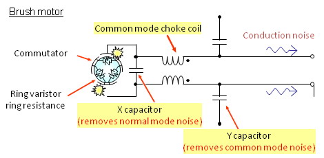 In the assembling of the motor additional grounding wires were connected to the internal motor chassis and the external motor chassis. Both were connected to the ground point of the deck chassis. This reduces the generated motor EMI noise. Additional external filter that uses common mode choke and X/Y caps was used to suppress the motor noise. A countermeasure for differential mode noise uses an across-the-line capacitor (X capacitor) that connects across two power lines.
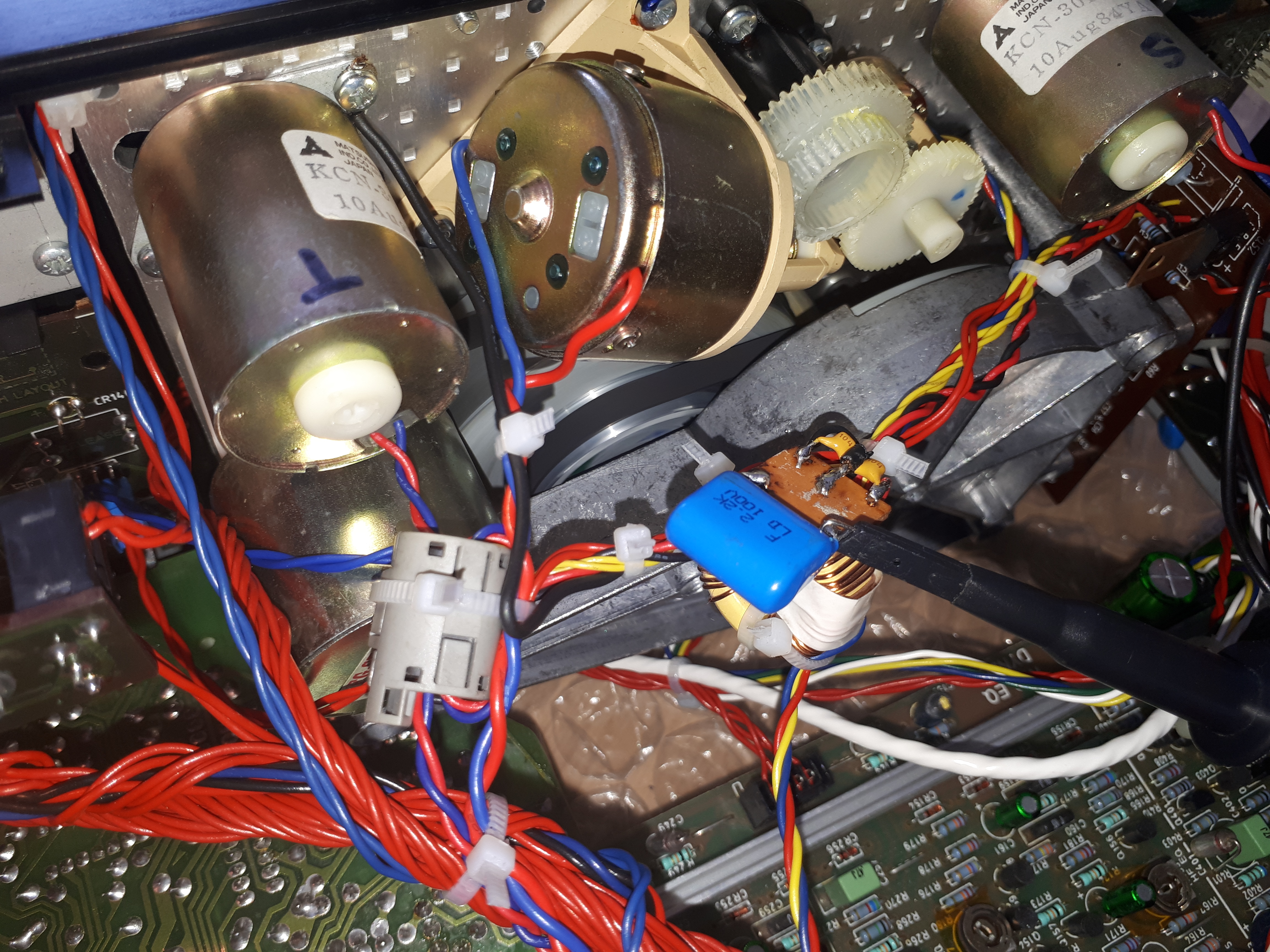 A countermeasure for common mode noise uses a line-bypass capacitor (Y capacitor) that creates a connection between both lines and a chassis ground. If the capacitor alone is not sufficient to suppress noise, the addition of a common mode choke coil can effectively suppress common mode noise that is otherwise difficult to overcome, and it is possible to take measures against even often problematic high-frequency noise. On the photo can be seen how the two filters for the take-up and capstan motor looks like. The gray choke use two winding of the twisted pair tape-up motor cable. It is enough to suppress the noise from the motor. The playback voltage of this motor is not so high due to the smaller torque required in play mode. The measured take up force is about 45g-cm. The Blue PP X cap is soldered on the choke board of the common mode filter. Small yellow ceramic caps are used as Y caps.
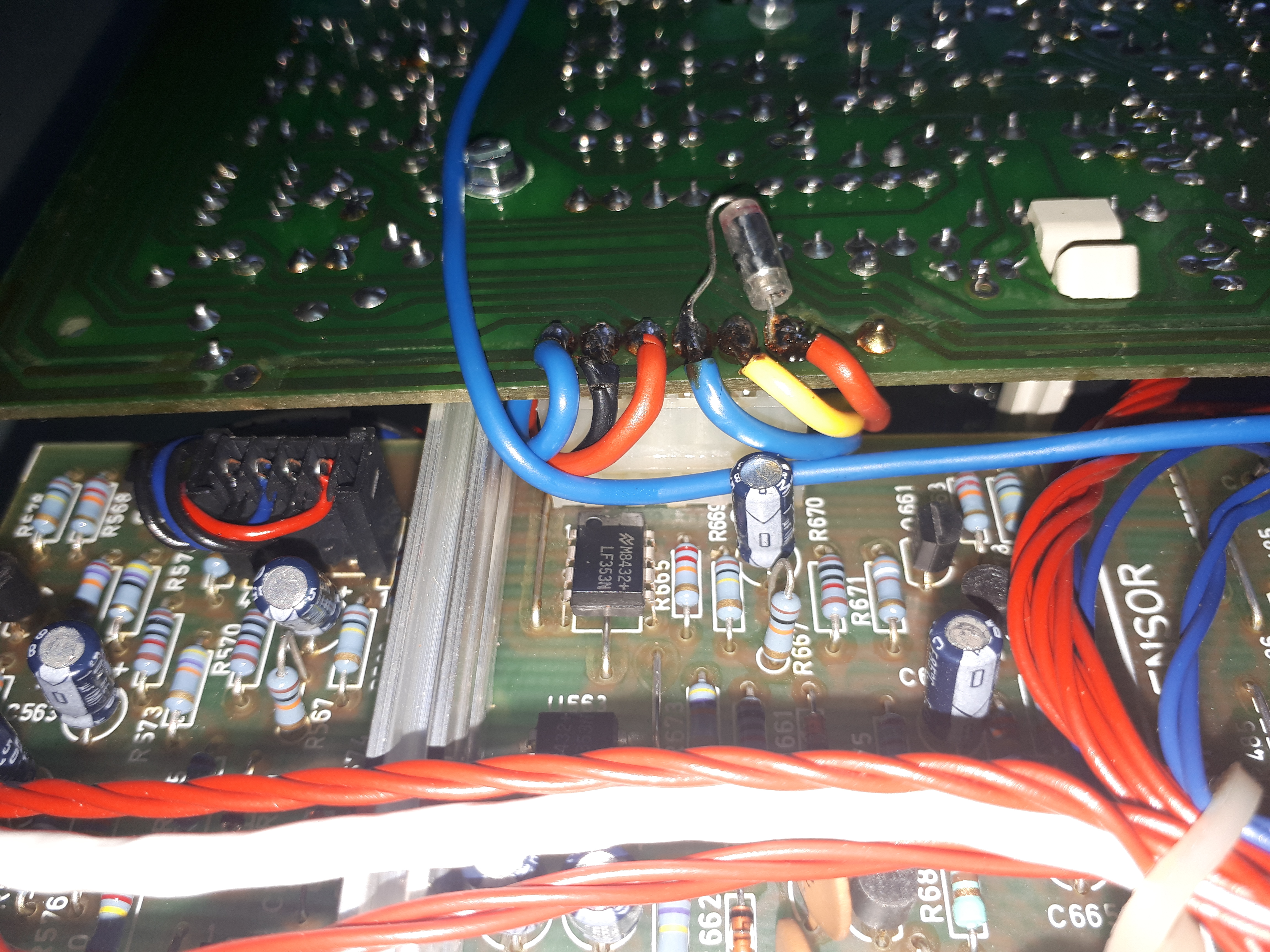
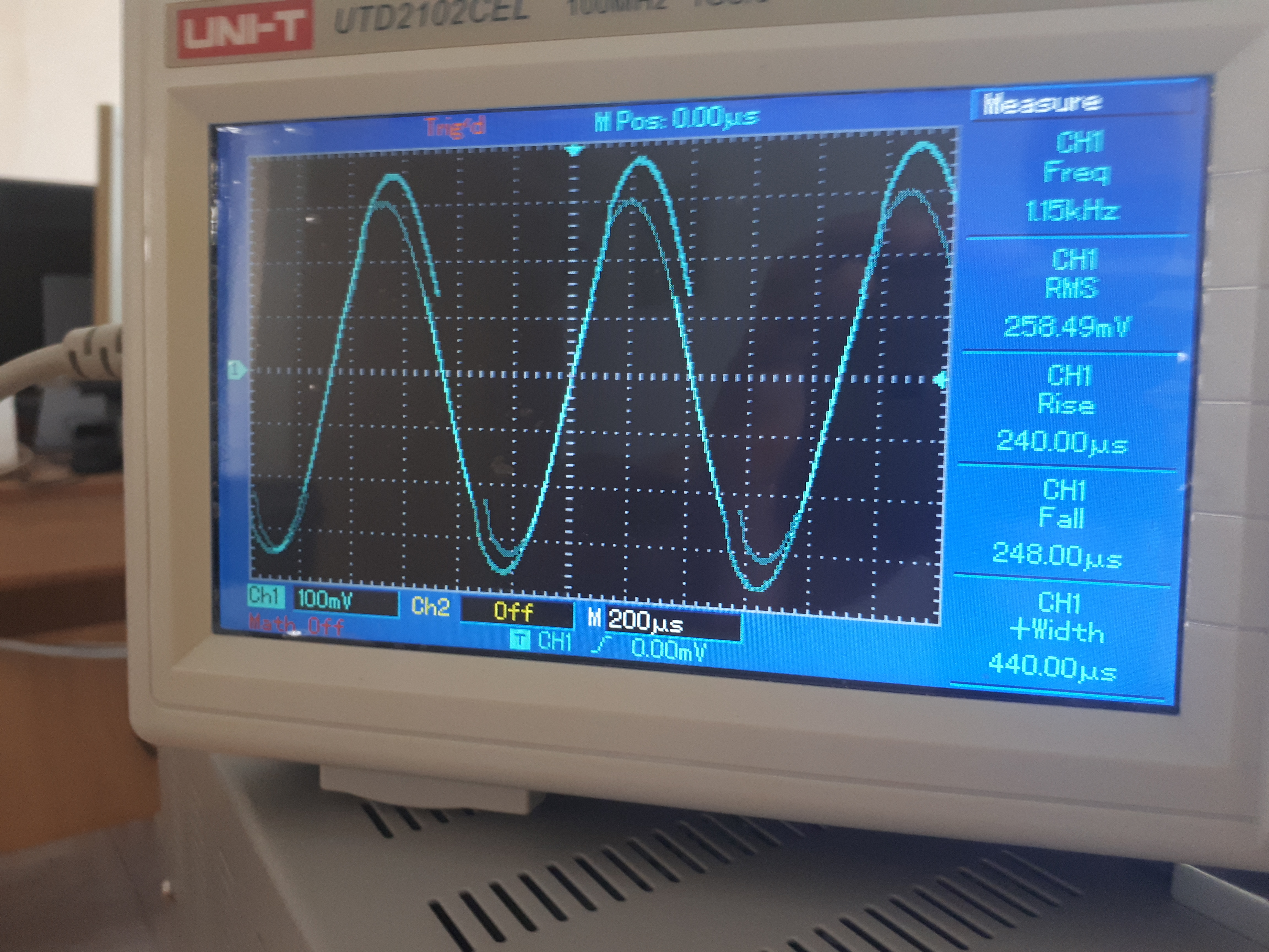
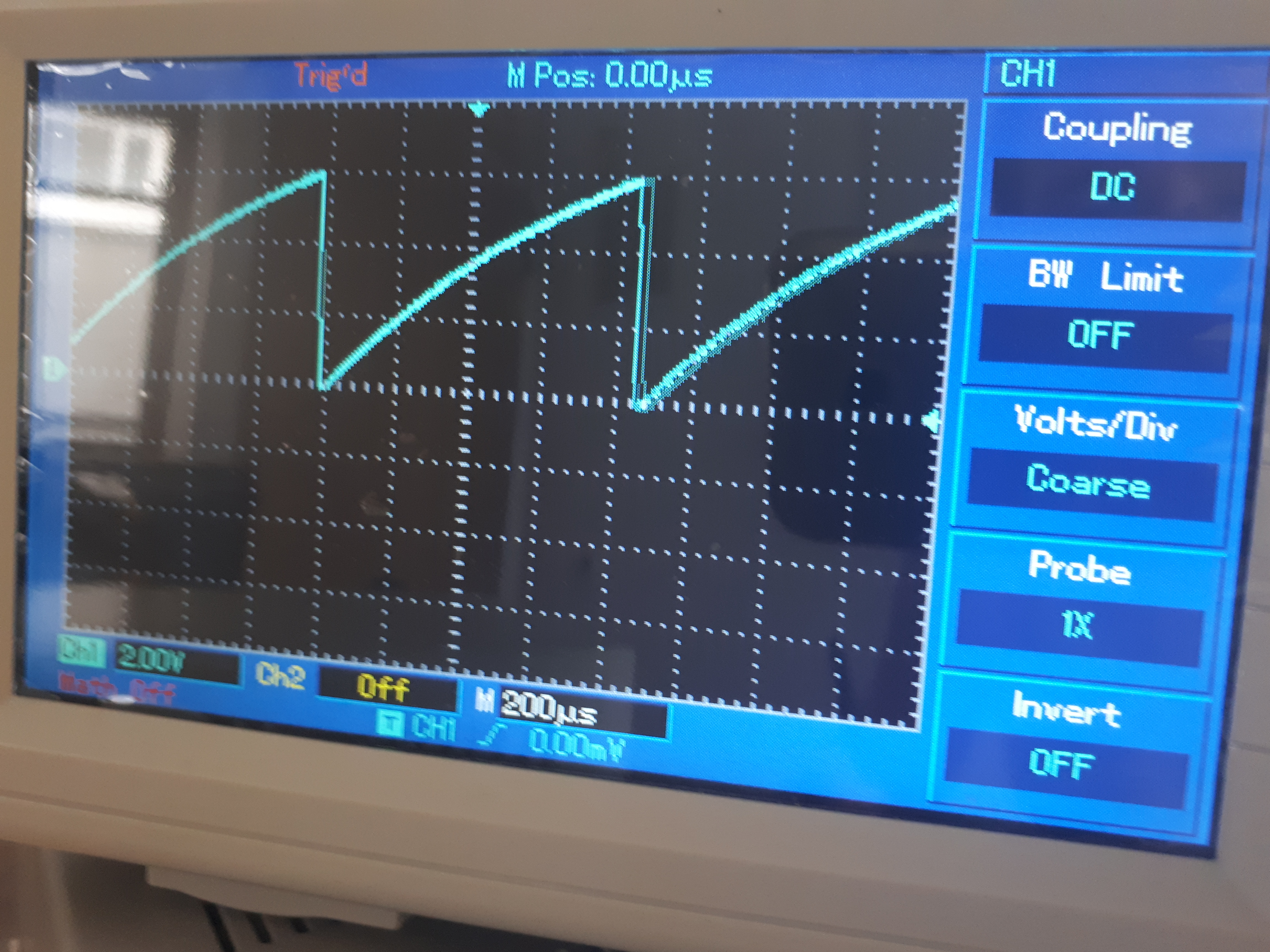
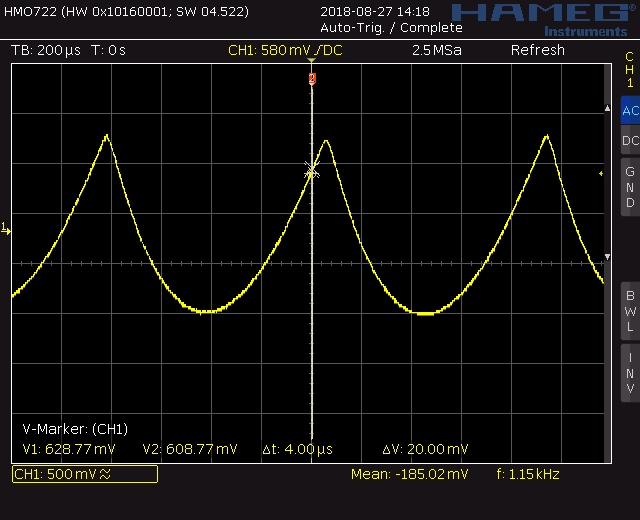
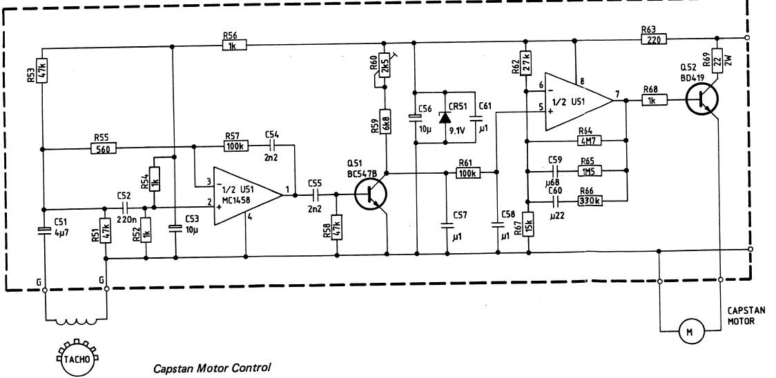 The motor regulator works stable. It consist of frequency to voltage converter and current buffer. We change the C53, and C56 to 100uF/25V. Another 100uF/25V caps was soldered in parallel to the power connector of the motor control board. Additional suppression diodes were soldered in parallel to the motor power terminals (anode to the emitter of the Q52) and another one suppression diode connected to the emitter and the positive power supply of the board (anode to the positive power supply). The waveform of the generated tacho signal is sine. The output of U51 (pin1) form a square signal proportional to the rotation speed and 50% duty cycle. Passing the C55 it form RC differentiator with a single peak, which cause the transistor to discharge the integration C57 capacitor (next photos represent the time chart of the signals). The ripple (in AC and DC mode) on the capstan motor can be seen on the bottom scope snapshots.
Some of the 3014 decks have speed regulation problem. Maybe 3 of the 5 decks that I serviced were out of regulation and increased speed. Still at the end position of the trim pot the speed was too high (~3200Hz instead of the 3000Hz measured with the test tape). The solution is to increase the value of the C57 in the range of 122-150nF. The easy way to do that is to solder additional 22nF PP cap in parallel to the C57. I suspect that the motor change its parameters in time and the regulation loop cannot follow its initial parameters. The speed regulation control did not use fixed comparison criteria. For example there is no reference frequency comparison module (PLL or quartz controlled comparator).
Part 4 – Conclusion & Measurement
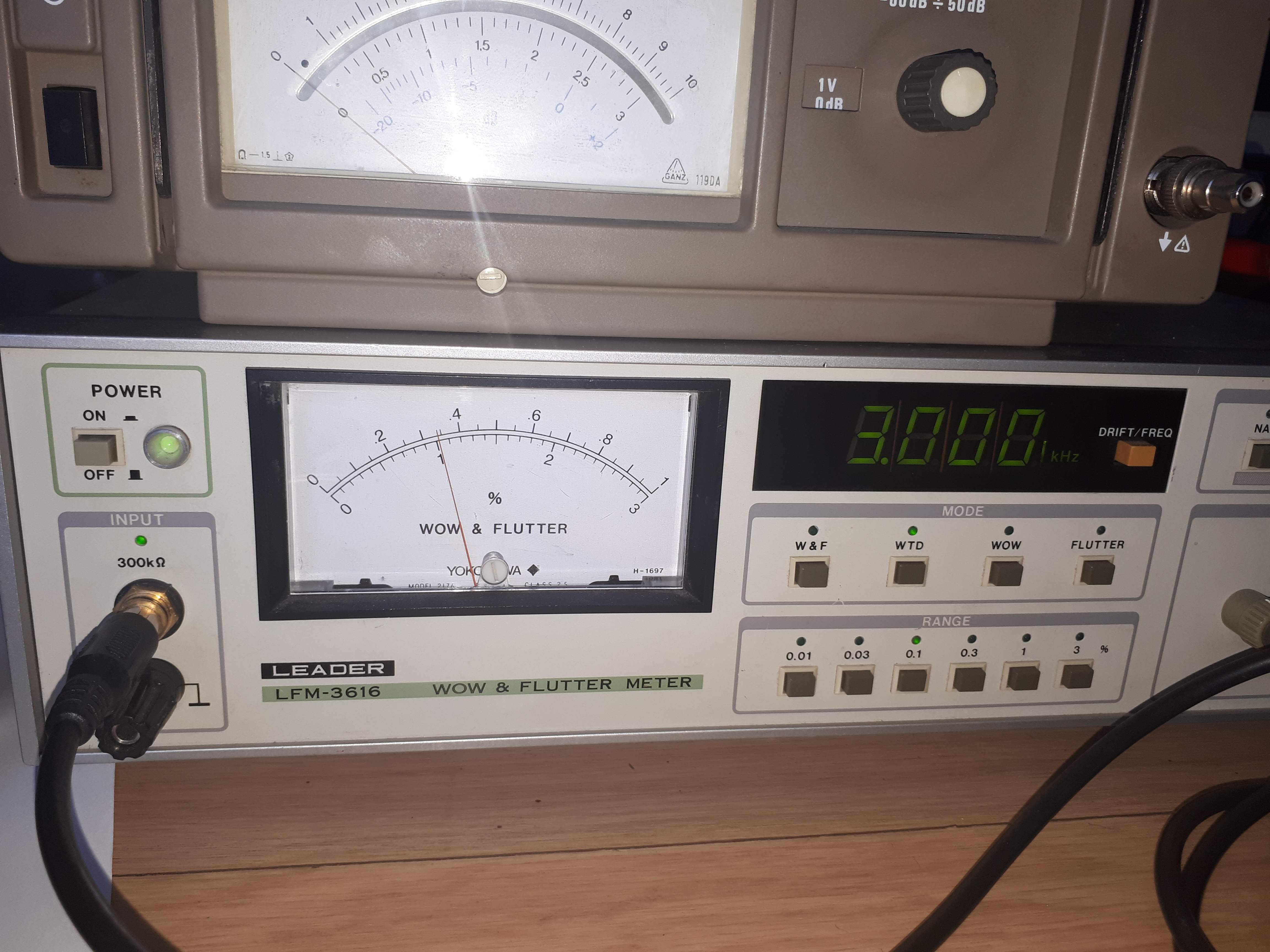 The measured W&F using ABEX and Sony test tapes show improvement of the final result after the repair. The factory specs are for 0.06% WTD. As can be seen the measured W&F is about 0.035% JIS WTD. The speed is smooth in time with very small frequency deviation. Azimuth was tuned using TEAC test tapes. Another check for playback frequency response was made using both MTT256 and MTT257H test tapes. The reference marks for 125Hz, 1kHz and 10kHz show the same level and that is another prove that the TCD-3014A is fully compatible with the IEC Prague 1981 standard. Recorded tape on 3014 was played back on the Nakamichi Dragon and confirms the frequency compatibility.
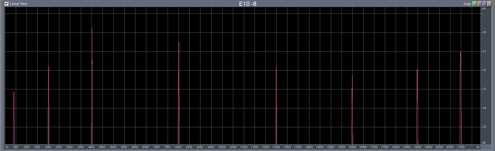 The recording frequency response was calibrated to be flat in range for TDK-D, Sony UX-Pro and TDK MA-XG tapes. The original frequency response show deviation in the range +/-3dB (can be seen in the level markers).
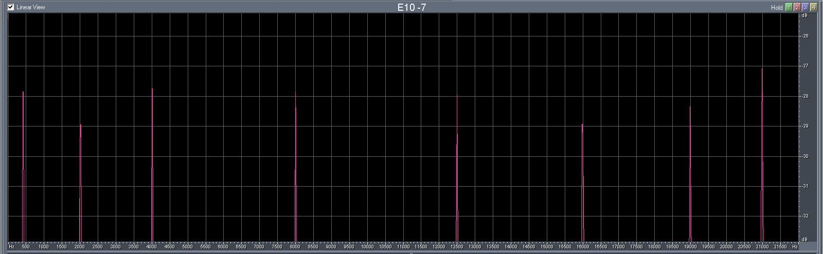 After the alignment the maximum deviation for most modern tapes is in range +/-1dB from 400Hz (the left marker, which is the reference point for comparison) up to 21kHz (the most right marker).
The service manual of the TCD3014 refer 700mV at the output (also Dolby test points) for reference zero dB level on the program meters. The service manual also notify that the Dolby level of the TP4 test point when use standard Teac MTT150 test tape is 580mV. A simple calculation can be done for the output voltage for the reference IEC level at 250nWb/m and the required voltage is about 665mV at the output. It seems that the zero db on the program meters on the 3014 is at higher level (+0.45dB compared to the reference IEC) but on the same time there is a full compatibility with the Dolby level. The headroom in the recording on the 3014A is very high. There is no noticeable listening distortions even up to +6dB on TDK-D tapes. That is why Tandberg decide to use higher reference level on the meters. Also there is no noticeable high frequency saturation on the tape due the DYNEQ system (dynamic high frequency equalization). It disable the HF boost EQ network in higher output levels. That acts like additional compression and prevents extremely tape saturation.
Some not so familiar functions in the TCD-3014A controls and program:
-
Real time counter is activated when insert new cassette and press the Set button. The program rewind the cassette to the beginning and scans it on playback mode for several seconds. Then the real time counter is activated.
-
Program search can be activated in stop mode. When holding the stop button and pressing the rewind or wind button together with the stop button several times depend on the song you need to find then the display show PC and a digit corresponding to the number of the song to be scan for.
-
In Wind or Rewind mode you can use two times slower speed by holding the wind or rewind buttons.
-
When the Rec Preset button is activated then the program meters show the input signal of the Line In monitor never mind the mode is Tape or Source in the stop mode. When the Play is activated then the program meter automatically show the playback level.
Part 5 – BOM list (Bill of Materials)
Power Supply Caps
————————
C869 – 6800uF/50V
C866, C865 – 5600/25V
C871, C872 – 1000/25V
C879, C880 – 2200/16V
C877, C878 – 100uF/25V
C870 – 5600/25V
C874 – 3300/6.3V
Other caps
————————-
C146, C148 – 100uF/25V
C567, C667 – 2.2uF/50V
C563, C663 – 1uF/50V
C567, C668 – 1uF/50V
C565, C665 – 1uF/50V
C161, C261 – 2.2uF/50V
C158, C258 – 2.2uF/50V
C324 – 100uF/25V
C1005, C1009 – 3300uF/6.3V
C1510, C1509, C1504 – 100uF/25V
C1402 – 47uF/63V
C1141 – 22uF/63V
C350, C450 – 1000uF/16V
C522, C622 – 1000uF/6.3V BP
C523, C524 – 1000uF/16V
C306, C406 – 1000uF/6.3V BP
C303, C304, C403, C404 – 820uF/16V
C119, C120, C219, C220 – 820uF/16V
C153, C253 – 220uF/6.3V BP
C354, C454 – 2200/16V
C1141 – 22uF/50V
C102, C202 – 820uF/16V
C104, C204 – 470uF/6.3V Elna Silmic II
C103, C203 – 470uF/6.3V Elna Silmic II
C101, C201 – 47uF/25V Elna Silmic II
C154, C254 replaced from 15nF to 3.3nF WIMA PP to fix the chrome tape FR on recording
C53, C56 – 100uF/25V
C51 – 4,7uF/50V
Transistor list for Input Amp:
———————————
Q101, Q201, Q103, Q203 – BC550C
Q102 – BC560C
Transistor list for Subsonic Filter:
———————————
Q117, Q217, Q118, Q218, Q122, Q222 – BC550C
Q116, Q216, Q119, Q219, Q123, Q223 – BC560C
Transistor list for Rec EQ:
———————————
Q151, Q152, Q251, Q252 – BC550C (matched)
Q154, Q254 – BC550C
Q153, Q253 – BC560C
Transistor list for Actilinear II:
———————————
Q301, Q302, Q401, Q402 – BC550C (matched)
Q303, Q403 – BC560C
Transistor list for Playback EQ:
———————————
Q354, Q355, Q454, Q455 – BC550C (matched)
Q353, Q453 – BC550C
Q351, Q451, Q357, Q457 – BC560C
Transistor list for Line OUT:
———————————
Q502, Q602, Q503, Q603 – BC550C
Q501, Q601, Q504, Q604 – BC560C
Transistor list for Headphone Amp:
———————————
Q522, Q622, Q523, Q623, Q534, Q634, Q529, Q629 – BC550C
Q521, Q621, Q524, Q624, Q535, Q635, Q531, Q631 – BC560C
First Dolby module:
————————-
C721, C730, C761, C771 – 100uF/25V, Panasonic FC
C753, C755, C713, C715 – 820uF/16V, Panasonic FC
C734, C767 – 220uF/6.3V BP
C775 – 10uF/50V
Q701 – BC560C
Q702 – BC550C
Second Dolby module:
————————-
C721, C730, C761, C771 – 100uF/25V, Panasonic FC
C753, C755, C713, C715 – 820uF/16V, Panasonic FC
C734, C767 – 220uF/6.3V BP
C775 – 10uF/50V
Q701 – BC560C
Q702 – BC550C
Mods Audio & Power chain:
————————–
100pF C0G/NPO capacitors in parallel to base-emitter of Q116
100pF C0G/NPO capacitors in parallel to base-emitter of Q117
100pF C0G/NPO capacitors in parallel to base-emitter of Q216
100pF C0G/NPO capacitors in parallel to base-emitter of Q217
100uF/25V to Q353 collector to ground
100uF/25V to Q453 collector to ground
100uF/25V in parrallel to CR392
100uF/25V in parrallel to CR393
100uF/25V in parallelo to C771 on both Dolby PCB
100uF/25V in parallelo to C772 on both Dolby PCB
10nF/PP cap in parallel to C306
10nF/PP cap in parallel to C406
10nF/PP cap in parallel to C303
10nF/PP cap in parallel to C304
10nF/PP cap in parallel to C403
10nF/PP cap in parallel to C404
10nF/PP cap in parallel to C324
10nF/PP cap in parallel to C153
10nF/PP cap in parallel to C253
10nF/PP cap in parallel to C101
10nF/PP cap in parallel to C201
Mods in Mecha/CPU control:
————————
1uF/50V BP in parallel to J1232 (mecha motor)
100uF/25V in parallel to J564 (capstan power)
470uF/25V between the emmiters of Q1235 and Q1236
470nF poly cap in parallel to R1219
Adding ferrite filter in take up motor cable
100nF ceramic capacitor in parralel to power pins of U1002
100nF ceramic capacitor in parralel to power pins of U1003
100nF ceramic capacitor in parralel to power pins of U1004
100nF ceramic capacitor in parallel to output and gnd of U561