The amplification of low signals from inductive transducers is not an easy task. Existing integrated amplifiers are good enough but in some applications the requirements are for better signal to noise ratio and high gain. For example the LT1028 / LT1128’s voltage noise is less than the noise of a 50Ω resistor. Here we are discussing the practical aspects for designing an ultra low noise preamplifier with input voltage noise less than 5Ω resistor, which is about 0.3nV/√Hz.
More technical details about this project can be found at the following paper, which may be useful for making new designs: LNA2104. The paper contain schematics and detailed explanation of the pre-amplifier. If you are interested in this project, you can request PCB kit. If you want, you can order this pre-amplifier as ready to use product or as kit version for soldering. All of the components are delivered by Mouser Electronics and they are not fake. For further details, please use the contact form of the site.
PCB DESIGN & PROTOTYPING THE LNA2104
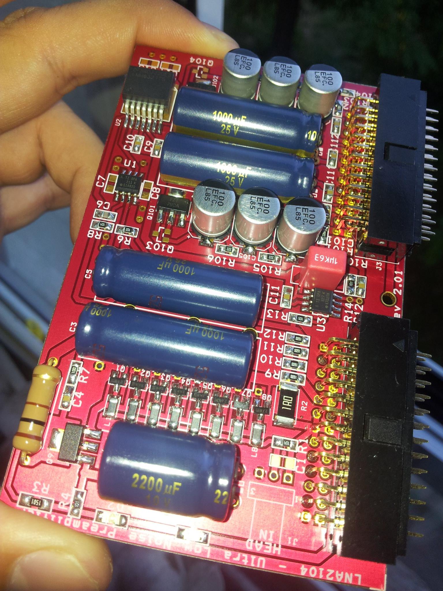 Design was made on double-sided PCB using ground planes on both layers. Ground planes are connected to the shield ground. The base material is FR4 with thickness about 1.55mm. The copper thickness is 55μm. The standard copper thickness is 35μm but it is very important to have low resistance tracks around the feedback network because of the low resistance of the feedback network. Most of the components are SMD. Wirewound resistors are the best choice for noise, followed by metal film, metal oxide, carbon film, and lastly, carbon composition. However, wirewound resistors are not readily available in large resistance values, and are usually inductive, which can cause instability problems in some cases. Many people prefer the “sound” of carbon comps, claiming they sound warmer than film or wirewound types. This is possibly due to distortions generated by the modulation of the contact noise current by the AC signal. Since this noise has a 1/f frequency characteristic (similar to pink noise), it is more pleasing to the ear than white noise. However, pleasing noise is still noise, and it should be reduced to the lowest possible level. Most people agree that carbon resistors are not suitable for cathode/emitter or source resistors. Although in some applications they are suitable for anode load resistors. That is because the cathode resistors are part of the local feedback which is very sensitive. The signal distortion is a different topic altogether. The electrolytic capacitors are based on the Panasonic FC Series Aluminum (105°C Low ESR) Electrolytic Capacitors. Some of them are SMD but the large capacitances are TH radial. The critical capacitors (C2, C5) are shielded with local metal folio cap, which is connected to the shield ground.
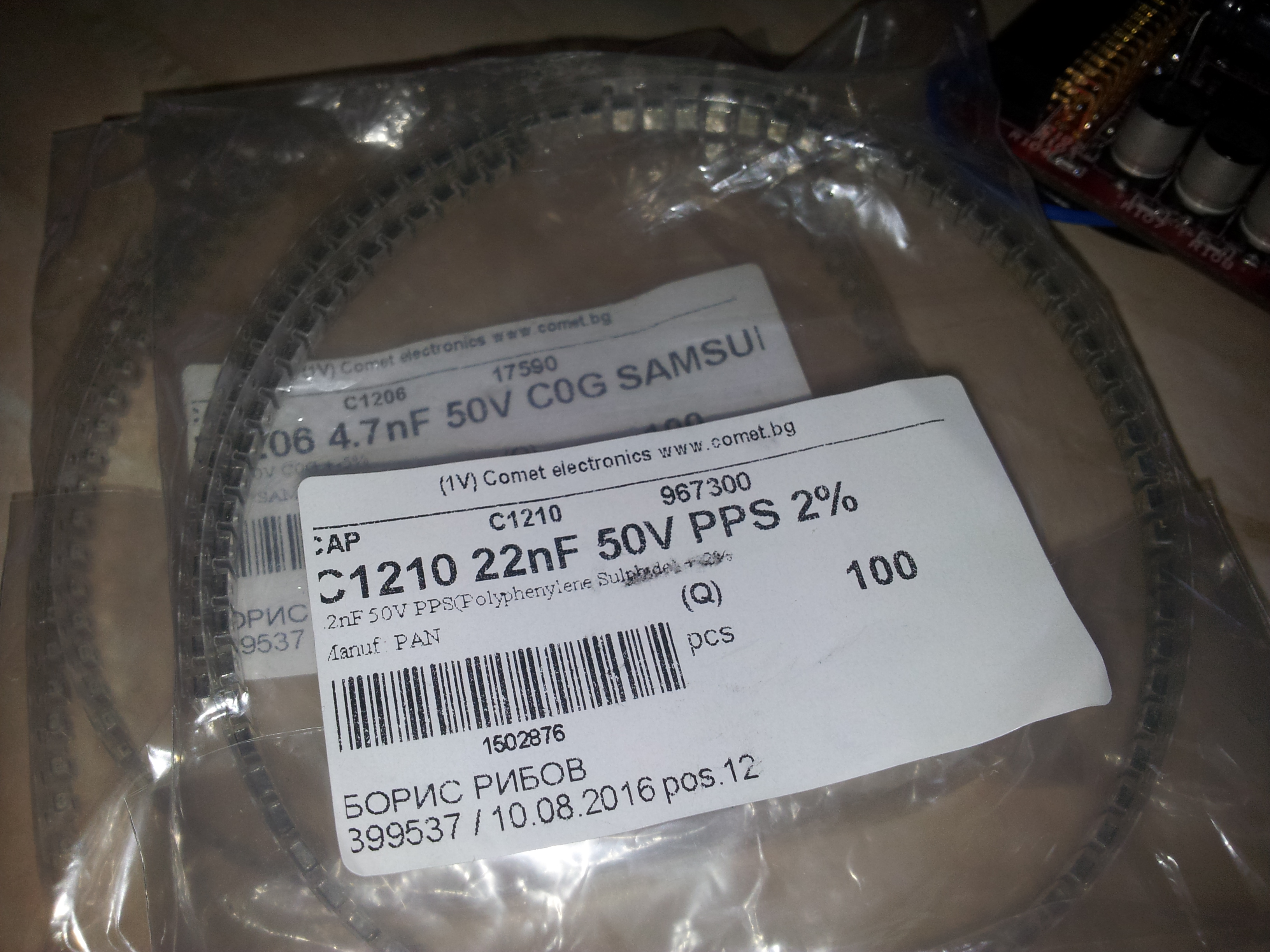 All Class-2 ceramic capacitors using ferroelectric ceramics exhibit piezoelectricity, and have a piezoelectric effect called microphonics, microphony or in audio applications squealing. Microphony describes the phenomenon wherein electronic components transform mechanical vibrations into an electrical signal which in many cases is undesired noise. Sensitive electronic preamplifiers generally use Class-1 capacitors to avoid this effect. So we used the Class-1 ceramic capacitors, NP0/CG/C0G. Their capacitance is limited to about 1-10nF for the 0805 footprint. For the capacitances about 22-100nF we used WIMA MKS2, also Panasonic Metallized PPS Film Chip Capacitors.
Routing of the board is very critical for the good final results. One urgent thing is to avoid the current loops. The JFETs are placed close each other. A shielding copper plane is placed on the bottom side of the board. The design implements tree different grounds. One is the shield ground plane on the top and bottom layer. Both shield grounds are connected together but are not connected to the signal and power ground. Power ground comes from the power supply connector and first it reaches the filter capacitors C109-C110. Common net from the capacitors is used as reference signal ground and is connected to the ground pin of the feedback resistor R2. The ground pin of the input signal is connected also to the R2. Ground pin of the R2 acts as a reference pint to the analog ground. The track that connects the source terminals of the JFETs is placed on the top layer. For this track it is important to be as short as possible, also to be with enough width to avoid voltage difference on the source terminals of the transistors. This track is shielded on the bottom layer.
PROJECT GOALS
- Eight parallel BF862 for the input stage. That approach reduces the equivalent input noise by square root factor of 8. So the equivalent input noise is 0.283nV/√Hz instead of 0.8nV/√Hz for a single transistor. Paralleling 8 JFETs increase the input capacitance and the Miller effect. The Miller effect accounts for the increase in the equivalent input capacitance of an inverting voltage amplifier due to amplification of the effect of capacitance between the input and output terminals. The virtually increased input capacitance due to the Miller effect is given by the product of the multiplication of the input capacitance and the gain of the stage plus one. Imagine that you have a gain of 1. The input signal at the output appears at the same amplitude but in inverse. The gate-drain capacitance is charged by the twice voltage product, so that its equivalent gate-drain capacitance doubles. This reduce high-frequency dynamics and the high-frequency response.
- High gain BJT (FZT690B) in the cascode configuration to reduce the Miller effect. This is done because the cascode works as common base with constant voltage to its emitter terminal. That reduce the drain capacitance multiplication. The collector load resistor of the BJT is only 100Ω, which allows the use of good bipolar SiGe amplifier with relative high input current noise on the second stage instead of precise expensive FET op-amp. We use OPA211 as the buffer amplifier with input voltage noise of 1.1nV/√Hz and current noise of 1.7pA/√Hz. FZT690B has a gain of 400 at 1A collector current. The measured noise of the transistor is 0.6nV at Ic=1mA and 0.38nV at Ic=10mA.
- Current feedback design (CFB) with low resistance of the feedback network. This design uses 39Ω to 1Ω, which ensures gain of G=40. This gain is good enough for amplifying the input low signals in the range of 1-4mV. The thermal noise from the 1Ω resistor is just 0.128nV/√Hz.
- High current buffer acts as a follower between the output of the OPA211 and the feedback network. Feedback network cannot be connected directly to the output of the OPA211 because of its current limit. The buffer is LMH6321 and has ability to supply ±300mA. This unity gain buffer has a voltage noise density of 2.8nV/√Hz and current input noise of 2.4pA/√Hz. The current noise is not important at all, because the buffer is connected to the low output impedance of the OPA211. The slew rate of the buffer is about 210 V/μS at 50Ω load.
- Power supply ripples cancellation circuit on pin 3 of U1. Even an extremely quiet power supply will still have something like 8nV/√Hz to 10nV/√Hz noise; under these circumstances, even with a local RC filter, achieving 0.3nV/√Hz is impossible (at least because a large electrolytic still has hundreds of milliohm impedance, not low enough to short the power supply noise voltage, usually with a much lower output impedance). By referring both op-amp inputs (in AC) to the positive power supply rail, the power supply noise is now appearing on the op-amp common mode, being therefore rejected through the op-amp CMRR. The overall head amp PSRR is down to better than -50dB.
- An inverting servo, built around an OPA827 JFET input op-amp is taking care of setting the OPA211 op-amp common mode voltage, so that the output offset is cancelled. That way the design removes all coupling signal capacitors.
- The power supply noise has to be filtered out. A standard emitter follower power buffer (capacitance multiplier) does a pretty good job, however there’s one thing that it can’t filter out: the emitter follower rbb’. To avoid that contribution, we need some sort of local feedback loop, to obtain a significant lower equivalent rbb’. This is easily achieved by using an Sziklai configuration for the emitter follower. By including the power device in a current feedback loop, its rbb’ is effectively cancelled. It’s now the low power device (which can be a low noise device) that dictates the equivalent rbb’ of the emitter follower. Divided by the head amp PSRR, this contribution is negligible.
CONCLUSION & RESULTS
The corner frequency of this low noise amplifier is remarkably low. This is another proof that BF862 is an excellent low noise JFET. The corner frequency is about 15Hz. The self-noise is around 4nV/√Hz at 10Hz and 1nV/√Hz at 40Hz. The level of harmonic noise (50Hz plus odd harmonics) is very low. This is a direct result of a compact SMD construction. The measured slew rate is about 40V/uS. The preamplifier was designed to operate at output level of 100mV RMS. The test shows significant overload ability. The output goes linear without clipping up to 6Vpp. The preamplifier is suitable both for high and low impedance sources because of its low input noise level (0.3nV/√Hz at 1kHz), which is better than most of the BJT.
This low noise amplifier will be used as a head preamplifier for a reference tape reproducer, which development was started at the end of 2015. Also this preamplifier will be used in the first stage of custom-made laboratory signal to noise meter. Adding precise a-weighted filter to the output will be the next task in the project.